Room-Temperature Quantum Processor Architecture
A heterogeneous photonic processor that performs quantum computation at standard operating temperatures — eliminating the cryogenic infrastructure that constrains every competing platform.
Quantum computing requires near-absolute-zero temperatures
Today's quantum computers depend on dilution refrigerators that cool processors to 15 millikelvin — colder than outer space. Each system costs $15–20M, consumes 25kW of cooling power, and takes months to install. The volumetric footprint of a multi-stage dilution refrigerator exceeds 42U rack specifications, requiring specialized facility modifications for load-bearing and liquid helium storage. In uncooled photonic circuits, thermo-optic refractive index drift (dn/dT) induces localized phase errors that collapse quantum visibility after just 50–100 gate operations — an impenetrable ceiling for deep-circuit algorithms.
Compute with light at 300K via heterogeneous 3D-stacked photonics
The HR-PSQA (Heterogeneous Room-Temperature Phase-Stabilized Quantum Architecture) integrates three material subsystems — LNOI logic, Si₃N₄ routing, and SiC spin-register memory — in a monolithic 3D-stacked semiconductor fabric. A distributed optical phase conjugation (OPC) lattice passively reverses accumulated phase distortion via four-wave mixing, bounding deterministic phase error to <0.1 rad and enabling logic depths exceeding 1,000 gates without cryogenic cooling. The result: a quantum processor that operates in a standard 19" server rack with 99.4% energy reduction vs. dilution-refrigerator systems.
System overview
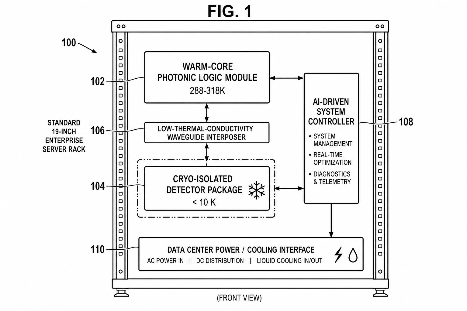
FIG. 1 — System diagram of the heterogeneous room-temperature phase-stabilized photonic quantum architecture illustrating thermal zoning between a warm logic core (288–318K) and cryo-isolated detectors (<77K) within a standard 19" enterprise server rack (100), with AI-driven system controller (108) and standard data center power/cooling interface (110).
LNOI Logic Fabric + Si₃N₄ Routing Backbone
The thin-film lithium niobate on insulator (LNOI) logic fabric utilizes the high Pockels coefficient of LiNbO₃ to execute sub-nanosecond gate operations with modulation bandwidths exceeding 100 GHz (a femtosecond piezo-actuator switch is a verification-pending upgrade path). The silicon nitride (Si₃N₄) routing backbone provides inter-chip optical transport at <0.1 dB/cm propagation loss with optical quality factors Q > 5×10⁵. Its 5.0 eV bandgap eliminates two-photon absorption at telecom wavelengths, serving as the primary optical bus between processing modules.
SiC Spin-Register Memory + OPC Lattice
Silicon carbide (SiC) spin registers utilizing VSi vacancy centers in isotopically purified 4H-SiC maintain coherence durations (T₂) exceeding 1.5 ms at 300K under CPMG dynamical decoupling protocols — providing on-chip quantum memory that eliminates off-chip fiber delay lines. The distributed mid-circuit OPC lattice (M=5–20 gate intervals) passively reverses linear phase distortion and chromatic dispersion via four-wave mixing in hybrid Si₃N₄/chalcogenide waveguides, bounding phase error to <0.1 rad independent of circuit depth.
Why this matters
Room-Temperature Operation
Operates at 288–318K (15–45°C). No dilution refrigerators, no liquid helium, no vibration isolation. Standard enterprise HVAC is sufficient. Thermal zoning confines only detectors to <77K via low-thermal-conductivity waveguide interposer while the entire logic core remains ambient.
CMOS-Compatible Fabrication
Built on commercially available silicon nitride photonics — the same platform used by Ligentec, AIM Photonics, and imec. Si₃N₄ core deposited via reactive sputtering below 400°C; chalcogenide overlay via thermal evaporation below 150°C. Full BEOL compatibility with no exotic materials for routing.
OPC Lattice Phase Stability
The distributed OPC lattice transforms phase-error scaling from unbounded linear growth to a bounded constant. After K OPC stages (~100 modules for a 1,000-gate circuit), total error is bounded independently of depth — no measurement, no ancilla qubits, no classical feedback required.
Quantum + Classical AI
The same LNOI logic fabric supports both quantum computation and photonic neural network inference (optical matrix-vector multiply). OPC modules maintain phase coherence across multi-layered interference matrices, preventing accuracy degradation. One chip serves two markets.
Standard 19" Rack Integration
Full system fits within 42U rack specifications with standard power/cooling interfaces. Co-locates with CPUs and GPUs for low-latency hybrid classical-quantum workflows. No specialized facility modifications, helium storage, or load-bearing upgrades required.
Sub-ns Electro-Optic Switching
Sub-nanosecond LNOI electro-optic switching (committed baseline) with >100 GHz modulation bandwidth — far faster than CMOS transistors; a femtosecond piezo upgrade is verification-pending. Clock rates exceed electronic components while maintaining single-photon quantum fidelity at the fundamental speed of light-matter interaction.
Key performance parameters
| Parameter | Specification | Significance |
|---|---|---|
| Operating Temperature | 288.15–318.15K (15–45°C) | Standard data-center HVAC; no cryogenic infrastructure |
| Logic Depth | >1,000 consecutive gates | 20× deeper than uncooled photonics without OPC (~50–100 gates) |
| Systemic Energy Reduction | 99.4% vs. dilution refrigerator | Eliminates 10+ kW/unit cryogenic overhead |
| LNOI Switching Speed | Sub-ns (committed); fs piezo upgrade verification-pending | Sub-nanosecond gate operations; far faster than CMOS |
| Modulation Bandwidth | >100 GHz | Exceeds electronic interconnect clock rates |
| Si₃N₄ Propagation Loss | <0.1 dB/cm | Ultra-low-loss optical bus for macroscopic chip distances >1 m |
| SiC Memory Coherence (T₂) | >1.5 ms at 300K | On-chip quantum memory; eliminates off-chip fiber delay lines |
| OPC Phase Error Bound | <0.1 radians | Deterministic bound independent of circuit depth |
| AI Telemetry Parameters | ~10 billion | Real-time feed-forward recalibration and timing control |
| OPC Lattice Interval | M = 5–20 gate components | Distributed correction without ancilla overhead |
Built on established science
Ultra-Low-Loss Waveguides
Si₃N₄ waveguides demonstrate <0.1 dB/m propagation loss in commercial foundries (Ligentec, imec, AIM Photonics). Wide 5.0 eV bandgap eliminates two-photon absorption at telecom wavelengths. Silicon photonics quantum computing on fully integrated 300mm process flow demonstrated 99.98% state preparation fidelity (Nature 641, 876, 2025).
40+ Years of Validation
Phase conjugation via four-wave mixing demonstrated in fiber telecommunications since the 1980s. On-chip OPC confirmed at -5 dB conversion efficiency (31.6%) in silicon waveguides for 160 Gbit/s signals (Aston/UCL, 2025). Hong et al. achieved -12 dB FWM in 13 cm Si₃N₄ (2021). QLT extends proven techniques to single-photon quantum applications.
Room-Temperature Quantum Memory
Room-temperature operation of silicon carbide divacancy electron spins with nuclear spin entanglement demonstrated on an integrated semiconductor photonics platform (Nature Communications 15, 10256, 2024). VSi centers in isotopically purified 4H-SiC provide T₂ >1.5 ms under CPMG dynamical decoupling at 300K. US Patent 10,347,834 established SiC spin-qubit integration.
3D-Stacked Semiconductor Fab
Monolithic bonding of LNOI, SiC, and Si₃N₄ layers uses established wafer-bonding and evanescent-coupling techniques. Modular photonic quantum computer comprising 35 chips linked by 13 km fiber across 4 server racks demonstrated at room temperature with 86.4 billion entangled modes (Nature 638, 912, 2025).
Connected patent architecture
OPC Waveguide
The hybrid Si₃N₄/chalcogenide nonlinear waveguide that performs four-wave mixing inside each OPC module — the physical engine of phase correction with γ_eff ~10–12 W⁻¹m⁻¹.
View Patent →Ultrafast Optical Switch
Sub-nanosecond TFLN electro-optic switches (committed baseline; fs piezo upgrade verification-pending) providing feed-forward routing, source multiplexing, and dynamic circuit reconfiguration within the HR-PSQA waveguide network.
View Patent →Stress-Relief Cladding
Mechanical stress management structures (isolation trenches, segmented overlays, polymer interlayers) ensuring OPC module reliability under -40°C to +85°C thermal cycling.
View Patent →Topological Photonic Circuit
Isotopically engineered topological PIC with piezoelectric actuation and monolithic quantum memory — an alternative circuit topology integrating with the HR-PSQA fabric.
View Patent →Periodic OPC Method
The method patent for distributing OPC modules at intervals of M=5–20 gates throughout the quantum circuit — the operational protocol for the processor's phase-correction lattice.
View Patent →Part of a 34+ patent fortress
This patent anchors QLT's Tier 1 Core Product IP. It is supported by specialized patents covering the coherence waveguide (Patent 02), optical switch (Patent 03), cladding structures (Patent 04), topological circuit (Patent 05), and periodic OPC method (Patent 08) — creating an interlocking mesh of claims that makes design-arounds prohibitively expensive.