GEMINI — Foundry PADP
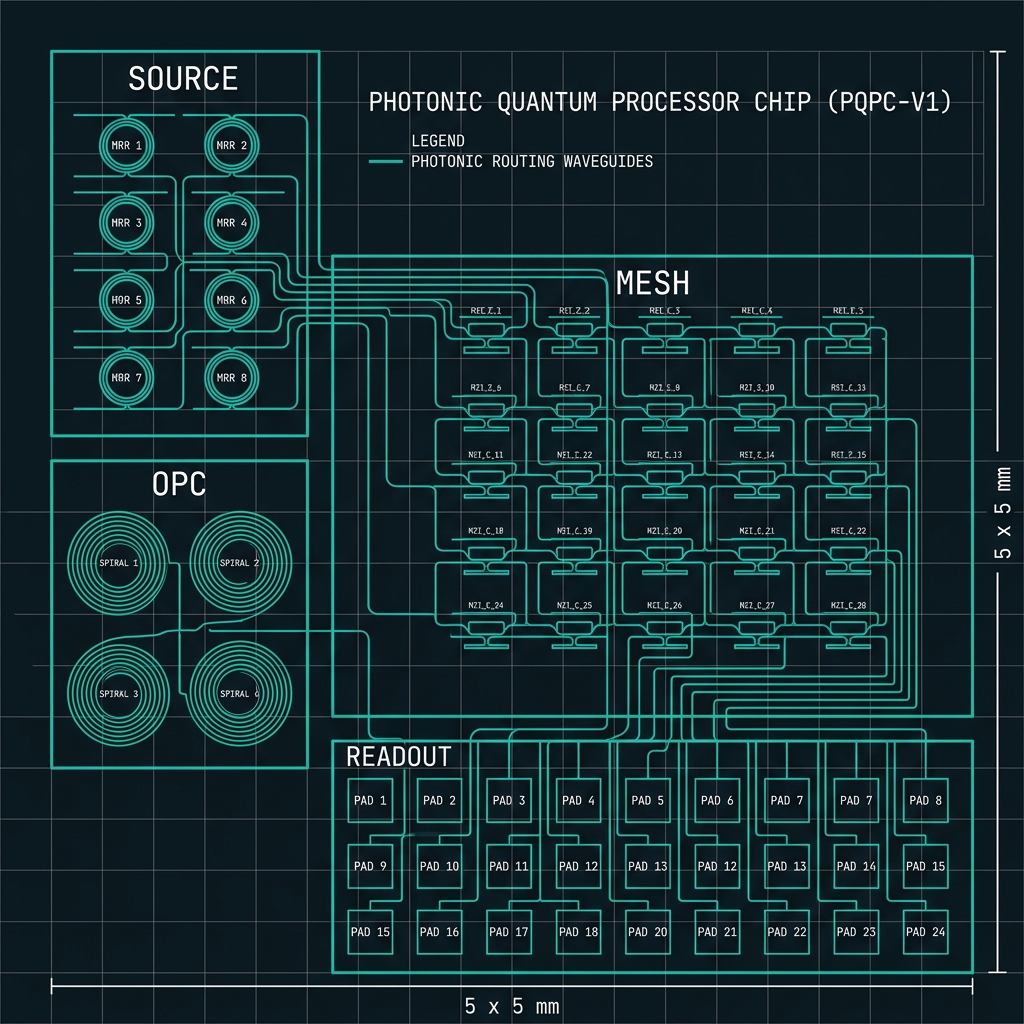
PADP submission package for QLT's only shipping-intent baseline: d=2 dual-rail path encoding on a 5×5 mm LIGENTEC AN350 die — 28 MZIs, 18 TFLN EO sites, 4 As₂S₃ OPC spirals, split-fab Phases A–D. Rev B2 · proposal-grade · no tape-out signoff claimed.
Platform summary
5 × 5 mm single die
Tiles: 1
< 0.5 W
CQFP butterfly
Detection stack
24 SPAD (8 herald + 16 mesh)
 F-G01
F-G01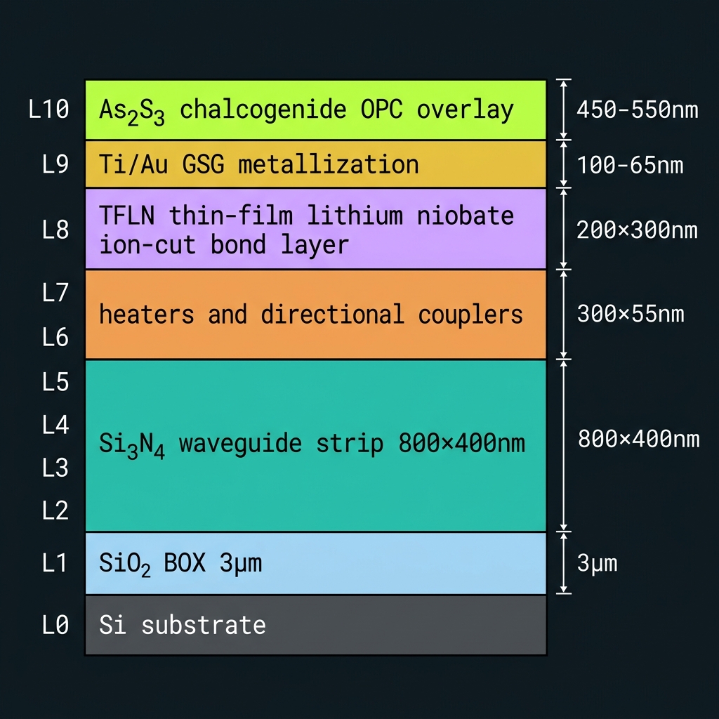 F-G02
F-G02Layer stack & materials
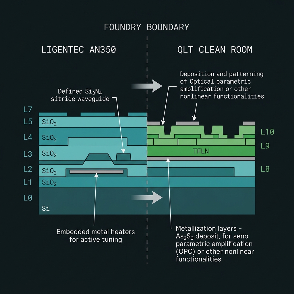
Shared L0–L11 platform across all eight PADPs — Si₃N₄ backbone, TFLN control, As₂S₃ LoCA BEOL (<210°C golden rule), optional AlGaAs MTP.
| Layer | Description |
|---|---|
| L0–L1 | Thermal SiO₂ BOX ≥ 3 µm on 200 mm Si |
| L2–L5 | LPCVD stoichiometric Si₃N₄ 800×400 nm strip; H₂ reflow @1150°C; upper clad + CMP |
| L6–L7 | Heaters, couplers, Clements mesh, LoCA windows (no OPC fill in foundry GDS) |
| L8 | TFLN ion-cut bond ≤500°C — 18 EO sites (16 switches + 2 phase rails) [QLT Phase B] |
| L9 | Ti/Au GSG + heater metallization ≤250°C [QLT] |
| L10 | As₂S₃ thermal evap 450–550 nm at 4 OPC sites; PECVD cap <150°C [QLT Phase C] |
StackDevice library
On-chip component inventory — status labels per R25 honesty audit.
| Device | Specification | Status |
|---|---|---|
| SFWM rings | K=8 heralded sources + rejection chains; no frequency comb on v1 | designed/target |
| Clements mesh | 28 MZIs · 32 thermo-optic heaters · 54 µs refresh | designed/target |
| TFLN switches | 16 feed-forward + 2 phase rails; >110 GHz BW class | designed/target |
| OPC spirals | 4 FWM cells (SITE-A×2 + SITE-B×2); η 0.5–2% CW cal. | claim/to-be-tested |
| Couplers I/O | Edge + grating; −3 dB GC / <−1 dB edge budgets | designed/target |
| Detectors | 24 SPAD bumps flip-chip; PDE ≥28% target | to-be-tested |
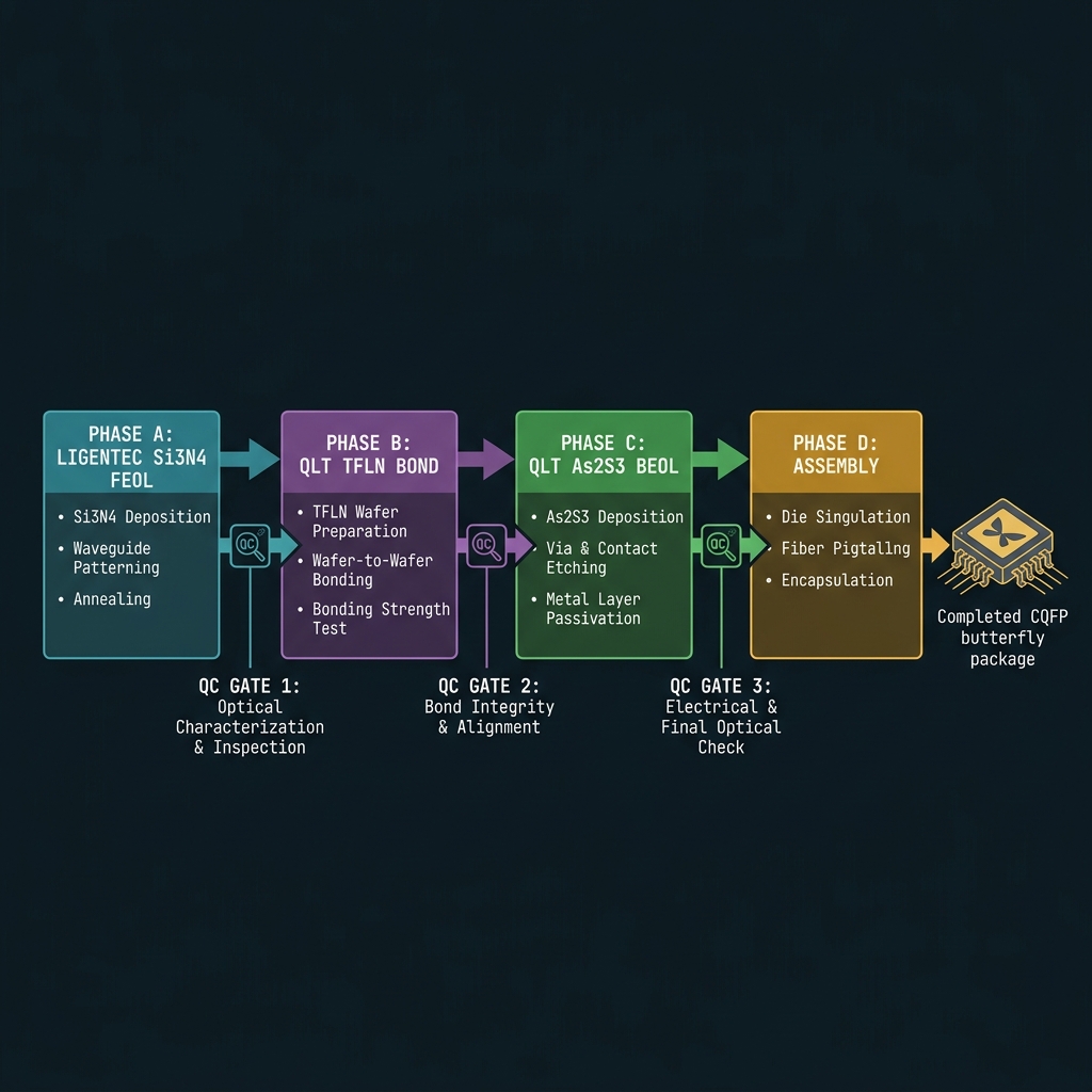
Split-fab phases & assembly
Ligentec FEOL → QLT TFLN bond → arsenic-isolated As₂S₃ BEOL → hermetic package. Foundry never sees arsenic, LN donor recipes, or full OPC geometry.
LIGENTEC AN350
L0–L7 Si₃N₄ FEOL
QC: Gate 0 DRC/LVS/MRC pre-tapeout
→ Planarized wafer or diced dies
QLT bond bay
L8 TFLN ion-cut bond ≤500°C
QC: Gate 1B bond yield + adiabatic IL
→ 18+ EO sites bonded
QLT arsenic BEOL
L9 metal + L10 As₂S₃ <210°C
QC: Gate 2 OPC G≥+2 dB classical
→ Processed dies with LoCA fill
QLT assembly
Dice · fiber · SPAD · seal
QC: Gate 3 packaged acceptance
→ Hermetic module + test report
Phase D: dice → facet polish → active fiber attach → Au wire bond (32 heaters + 16 RF GSG) → flip-chip SPAD → hermetic seam-seal. v1 de-risk option: populate L0–L9 only, defer L10 As₂S₃ to follow-on lot.
 Assembly
Foundry requirements & intake gates
What the foundry receives vs. what QLT retains. Partial GDS via encrypted transport.
| Item | Requirement / status |
|---|---|
| Primary foundry | LIGENTEC AN350 MPW (X-FAB Erfurt 200 mm) |
| Backup | AIM Photonics — dual-qual non-blocking |
| GDS status | Partial GDS v0.1 — encrypted transport; OPC geometry withheld |
| DRC | 466 campaign flags dispositioned in dry-run rollup — no foundry signoff |
| Intake gates | NDA/DKLA · Gate 0 DRC/LVS · probe traveler · package ICD · ATP matrix — all Open |
Campaign intake gates (all chips)
| Gate | Requirement | Status |
|---|---|---|
| Intake checklist | 00-FOUNDRY-INTAKE-CHECKLIST.md completed per chip/foundry | Open |
| NDA / PDK | DKLA executed; active rule deck downloaded and versioned | Open |
| Gate 0 | Partial-GDS export, DRC/LVS, Q-layer strip audit, SHA-256 hash | Open |
| Wafer probe / KGD | Per-die disposition traveler (mandatory NOVA+) | Open / N/A |
| Package ICD | Fiber, electrical, thermal, mechanical interfaces as drawings | Open |
| ATP / OQC | Acceptance matrix, soak, fiber pull, hermetic/leak tests | Open |
| Foundry acceptance | Module order, waiver list, COA format, quote in writing | Open |
Open items FQ-01–FQ-08 centralized in 00-FOUNDRY-INTAKE-CHECKLIST.md §9. PDK assumption freeze (AN350/AN800 layer integers, LoCA limits, CD/overlay) is a hard hold before GDS upload. Partial-GDS boundary must be DRC-debuggable without releasing withheld As₂S₃/TFLN/AlGaAs/control maps.
Five-volume structure
Full specs in Foundry Chip Docs/GEMINI/QLT-GEMINI-PADP-Vol-*
| Volume | Title | Research memos |
|---|---|---|
| Vol I | System Architecture | R01–R04 · blocks, encoding, I/O, power/thermal/package |
| Vol II | Physical Architecture | R05–R09 · layer stack, TFLN, LoCA, floorplan, thermal/electrical |
| Vol III | Device Library | R10–R16 · rings, AWG, mesh, couplers, modulators, OPC, detectors |
| Vol IV | Foundry Requirements | R17–R20 · Ligentec/AIM matrix, custom modules, DRC/IP |
| Vol V | Simulation & Tape-Out | R21–R25 · sim plans, GDS roadmap, honesty audit |
Tape-out readiness & honesty audit
Vol V defines Lumerical/COMSOL/INTERCONNECT campaigns — status=planned. G1–G5 schematic figures generated; no fabricated silicon bench data. Critical path: T9 heralded HOM on OPC (RK-01).
No fabricated simulation results are claimed in Vol V — all campaigns status=planned. No GDS beyond v0.1 heritage layouts. No foundry DRC signoff. Promotion path requires closing gates in GEMINI-PADP-ROLLUP.md.
 F-G03
F-G03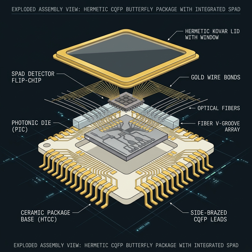 F-G04
F-G04Cross-links
Foundry Chip Docs · Rev B2
On-disk package: Foundry Chip Docs/GEMINI/ · Bundle: _export/QLT-PADP-RevB2-2026-06-11.zip