STAR-PHASER SOLAR
The roadmap chip that implements a structured d = 10 = 2 × 5 tensor-product composite — two orthogonal spectral subspaces (2-bin parity lane × 5-bin digit lane) carrying ℤ₁₀ decimal arithmetic and human-readable spectral symbols. Explicitly not GF(10), not algebraically closed. Bridges GEMINI dual-rail control to GALAXY field-native GF(16) in Region I (Q ≪ 0.2).
SOLAR specification table
One photon, one spatial mode — decimal digit via structured spectral encoding.
| Parameter | SOLAR value | Status | Notes |
|---|---|---|---|
| Brand / codename | STAR-PHASER · SOLAR | Roadmap | Post-GEMINI, pre-GALAXY epoch |
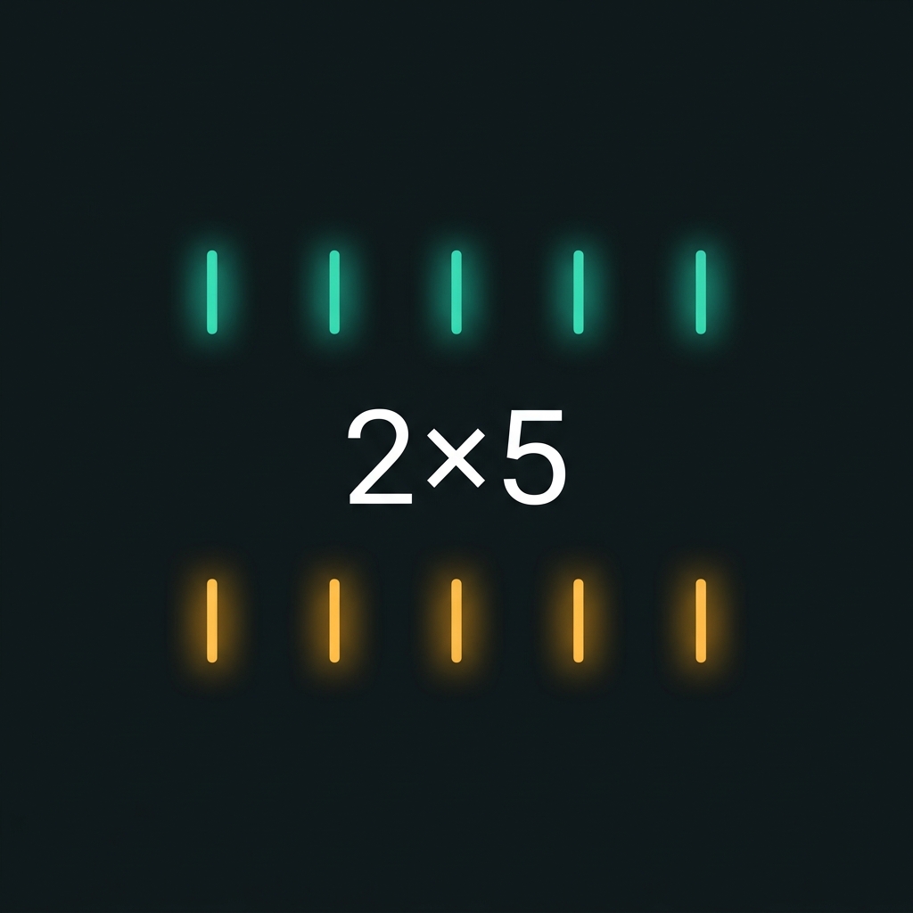
| Logical dimension | d = 10 = 2 × 5 | Designed | Structured composite qudit — parity ⊗ symbol |
| Algebraic structure | ℤ₁₀ ring | Model | Not GF(10) — 10 is not prime power |
| QUASAR region | Region I | Designed | Q = (H_NL + H_OPC + H_CV) / H_linear < 0.2 |
| Bits / photon | log₂10 ≈ 3.322 | Model | One decit per photon |
| Bin spacing Δf | 50 GHz | Designed/target | WS13 Δf table; gate-native RF |
| Comb span Bcomb | 450 GHz | Model | 9·Δf; two 5-tooth clusters + guard |
| OPC margin @ 12 THz | ≫ (27×) | Claim | Single-pass multi-bin conjugation |
| Phase pairs | 90 | Model | N(N−1) for N=10 |
| Gate engine | DQFP + SDCLA | Roadmap | EOM + shaper QFP cascades |
| Readout | 10-ch WDM or 5+2 staged | Designed/target | SPAD array; detection gates product |
| Successor | GALAXY · GF(16) | Roadmap | First clean field-native chip |
Eight expandable sections
Tap any tile to expand. Each section includes a How we do it implementation note.
SOLAR architecture
2×5 composite · ℤ₁₀ · Region I2×5 tensor-product encoding
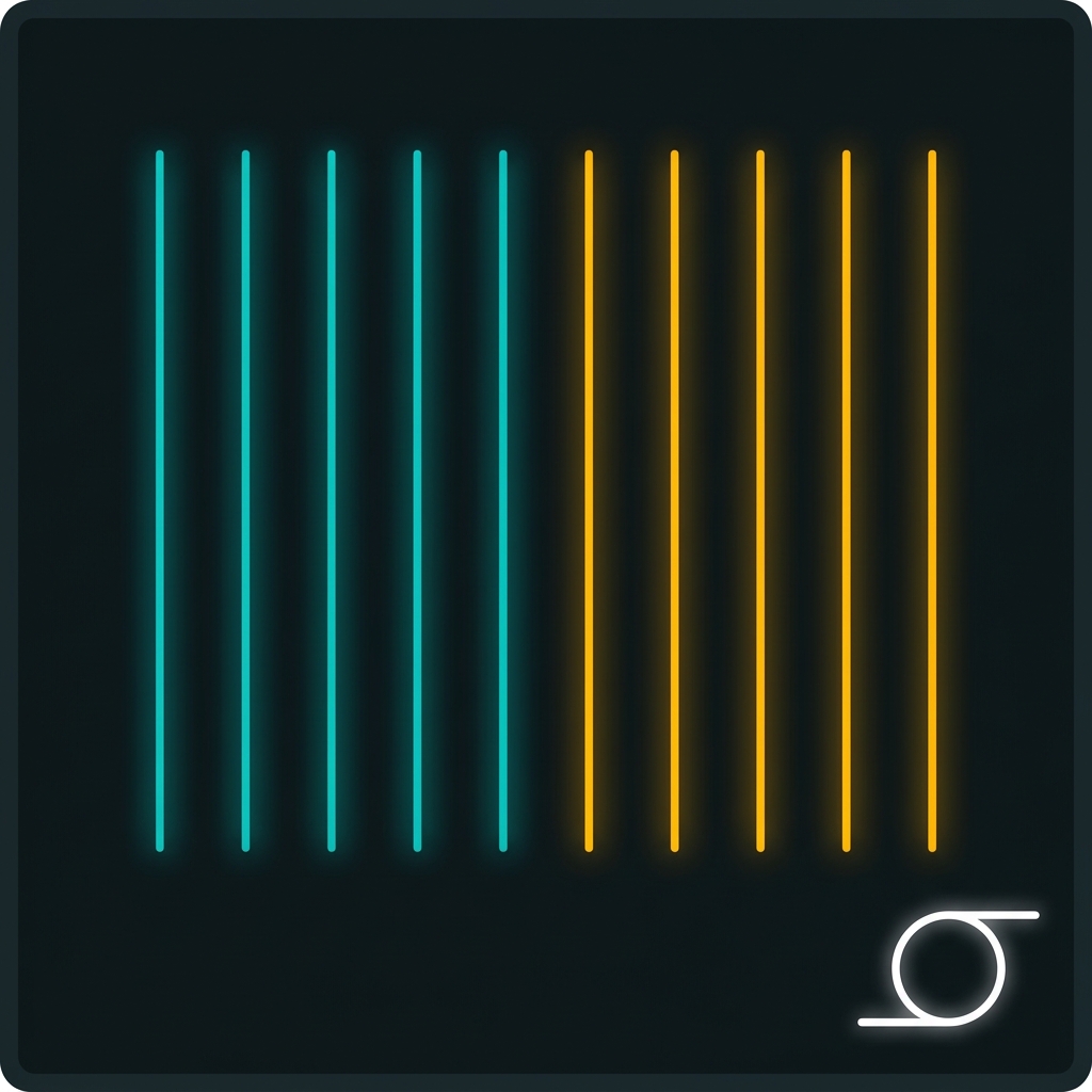
→SOLAR encodes one decit as |ψ⟩ ∈ ℂ² ⊗ ℂ⁵ — a parity subspace (2 levels) times a symbol subspace (5 levels). Decimal digit d = 5p + s where p ∈ {0,1} selects sub-band and s ∈ {0,…,4} the tooth within it.
Sub-band p=0 (digits 0–4):  f_{0,s} = f_ref + s·Δf
Sub-band p=1 (digits 5–9):  f_{1,s} = f_ref + Δf_guard + s·Δf
Δf = 50 GHz · Δf_guard ≥ 100 GHz
An engineer with an OSA sees two clusters of five lines — left cluster reads 0–4, right reads 5–9. This is intentional symbolic transparency, unlike GF(64) NOVA where 64 teeth are an algebraic grid.
Critical honesty: ℂ¹⁰ ≅ ℂ² ⊗ ℂ⁵ as vector spaces, but ℤ₁₀ addition does not factorize — DADD must respect carry across the (p,s) boundary (e.g. 4+7 flips parity).
How we do it: Mask two 5-ring shaper banks on the shared SiN bus; firmware LUT maps DQFP |d⟩ ↔ physical (p,s) amplitudes; publish spectral legend card on bring-up.
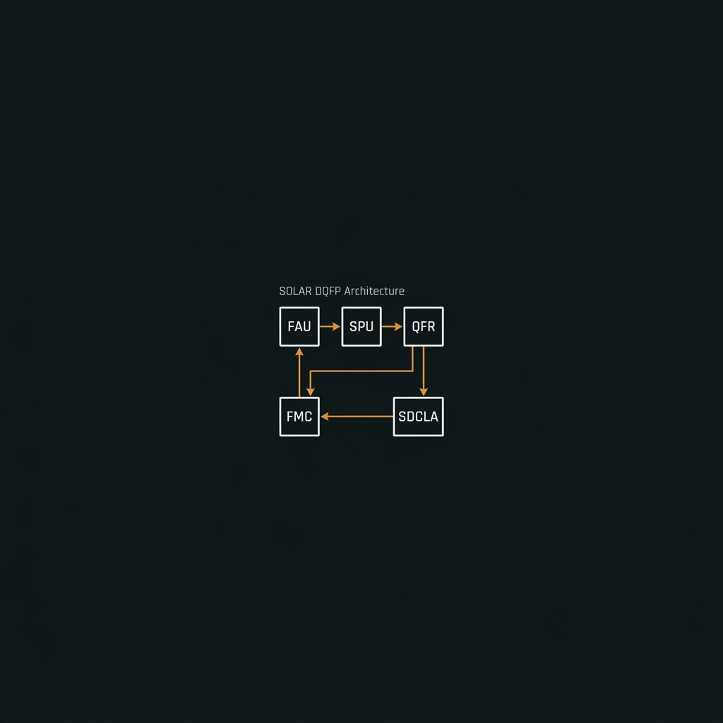
DQFP / SDCLA gate set
→SOLAR executes Spectral Decimal Computing (SDC) through the Decimal Quantum Frequency Processor ISA compiled to EOM+shaper QFP cascades:
- FAU — DADD, DSUB, DMUL, DDIV (mod-10 ring arithmetic)
- SPU — PHASE (Z₁₀), DFT10, IDFT10 on dual 5-ring shaper banks
- QFR — FSHIFT, FCYCLE, SWAP10, ENTANGLE10
- SDCLA — O(log₁₀ N) decimal carry via spectral Gᵢ/Pᵢ cells
- FMC — LOAD, STORE, COPY via SFWM comb memory
Primitives: X₁₀ (shift), Z₁₀ (phase), F₁₀ (decimal QFT). Identity F₁₀ X₁₀ F₁₀† = Z₁₀ is the algebraic backbone of Fourier-basis DMUL.
ℤ₁₀ limits: no GF(10) inverse (2⁻¹ mod 10 undefined); no char-2 XOR-add; no native RS/BCH — defer to GALAXY GF(16).
How we do it: Port G05–G11 ISA to 2×5 compiler backend; tensor ops emit band-local vs cross-band tags; OPC node after every 3–5 cascade stages bounds phase error.
10-tooth comb source & B07 fab
→A SOLAR decit begins as ten phase-coherent spectral lines from one pump via SFWM on a high-Q Si₃N₄ microring — same physics as Kues D=10 [demonstrated external].
Fab stack (B07): inserts into Steps 01–06 of manufacturing.html — SiN passives (comb ring, AWG, shaper rings), TFLN bond for EOMs, As₂S₃ OPC overlay post-bond (<210 °C golden rule). SOLAR is a subset mask of GALAXY/NOVA comb tiles, not a one-off chemistry experiment.
2×5 spectral shaping: pump detuning targets two five-line clusters rather than ten uniform adjacent lines — reduces adjacent-channel crosstalk during lock.
How we do it: Tape out comb ring + dual 5-ring shapers + AWG + microring bank; bond TFLN EOM via wafer-scale direct bond; deposit As₂S₃ OPC only at encoding-boundary sections; run T-B07 experiments 1–5 at d=10.
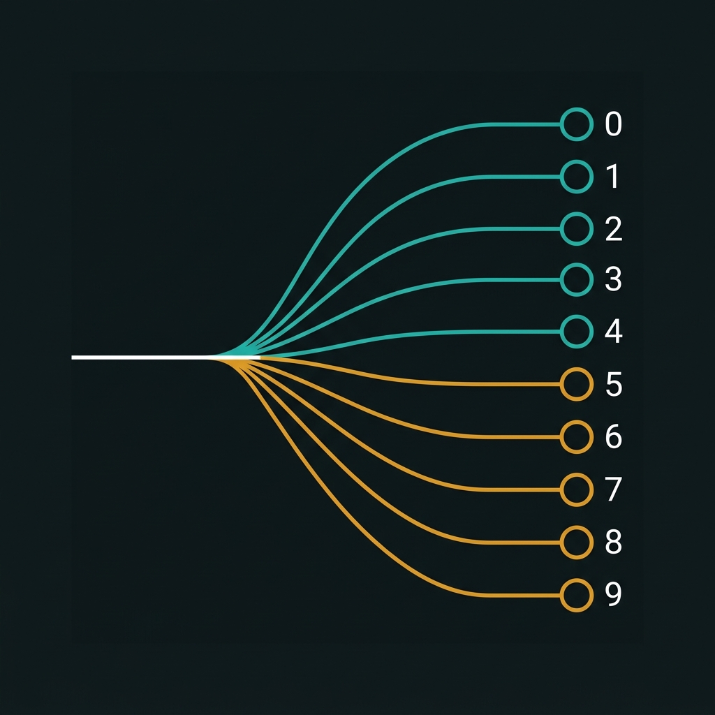
10-ch WDM routing & readout
→After DQFP compute, SOLAR resolves which decimal digit was stored via spectral routing:
- Parallel — 10-ch AWG or 10-ring demux → 10 SPADs (single-shot read)
- Staged 2×5 — parity discriminator + 5-ch demux per band (7 effective channels)
- Project-then-detect — QFP unitary → 1 demux → tomography / gate cert
B09 honesty: 10-ch demux crosstalk and SPAD calibration are the true gating risks for base-10 — explicitly not OPC bandwidth. Target F_read ≥ 0.98 on interior bins at ε ≤ 1% crosstalk.
How we do it: Place AWG + microring demux on mask (dual-variant strategy); calibrate confusion matrix C classically; implement 5+2 staged firmware aligned to S12 legend; wire 10 SPAD channels at package.
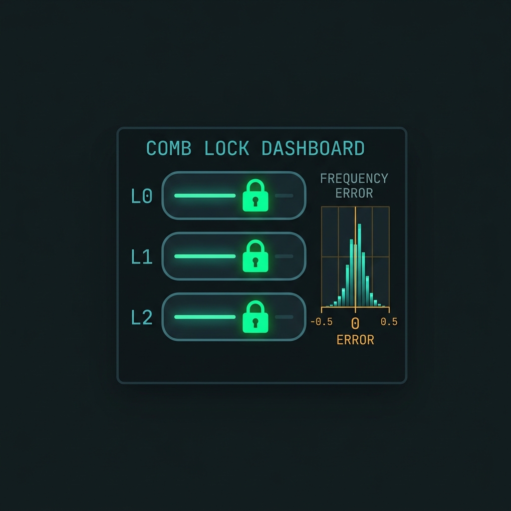
10-tooth comb lock
→Wafer resonance scatter (5–15% of FSR) misplaces teeth off the 50 GHz grid. Comb lock makes frequency labels trustworthy — without it, the human-readable spectral map is fiction.
L0 Global TEC        → ±5 GHz coarse
L1 Band coarse (2×5) → align Δf_guard between parity clusters
L2 Per-tooth (10)     → |Δf_err| < 0.5 GHz via TED heaters
grid_valid BOOL gates DQFP issue logic — compute stalls if FALSE. SOLAR is the low-channel-count shakedown for NOVA's 64-tooth lock (G47 scaled down).
How we do it: Integrate 13 heater channels with thermal-isolation trenches; port G47 firmware to 10-tooth / 2-band instance; implement independent TED matrices per 5-ring bank; lock target < 30 s per die at room temp.
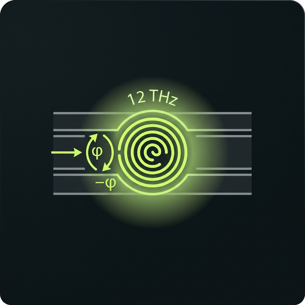
OPC at encoding boundary
→Region I SOLAR uses OPC as boundary correction, not distributed field computing. One broadband As₂S₃ FWM pass conjugates φ→−φ on all ten colors simultaneously — 12 THz ≫ 450 GHz (≈27× margin).
Boundary map: GEMINI→SOLAR transcode output; sub-band A↔B midpoint; post-QFP every 3–5 stages; pre-demux readout. Optional decit squeeze bridge (G25) narrows inter-bin Δφ between major QFP stages — CV-assisted DV, not GKP logical encoding.
Never-state: OPC corrects phase only (~3 dB/pass loss remains); it does not replace qudit QEC.
How we do it: Localized As₂S₃ patches post-TFLN bond; pump at band center of 450 GHz span; demonstrate single-photon OPC on dual-rail first (A104 §5), inherit to 10-bin; feed Z-bias metrics to qudit decoder co-model.
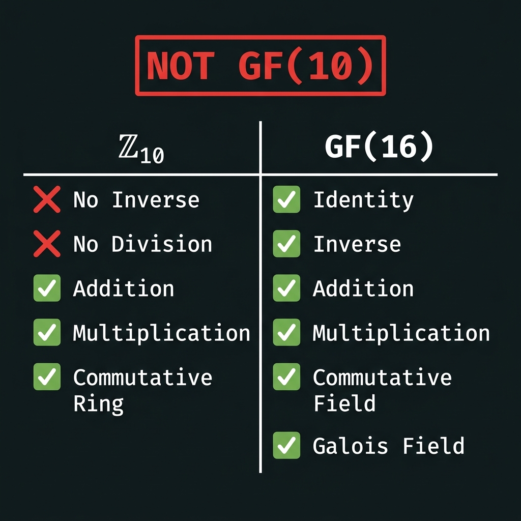
ℤ₁₀ arithmetic & QEC posture
→Investors routinely conflate "d=10 qudit" with "GF(10) field element." SOLAR explicitly breaks that conflation.
- Native decimal digits 0–9 — yes
- Addition / multiplication mod 10 — yes (ℤ₁₀ ring)
- Every nonzero element has inverse — no (zero divisors {2,5})
- Reed–Solomon over GF(10) — no (GF(10) does not exist)
QEC menu: Option A — ℤ₁₀ qudit codes (immature literature); Option B — prime-power engine + decimal I/O; Option C — OPC + embedded qubit surface code; Option D (recommended) — defer mature QEC to GALAXY; SOLAR = pre-QEC validation chip.
How we do it: Chip page banner states ℤ₁₀ not GF(10); software ABI exposes DMUL/DADD as mod-10 with zero-divisor documentation; no GFINV opcode; customer migration doc to GALAXY when field QEC needed.
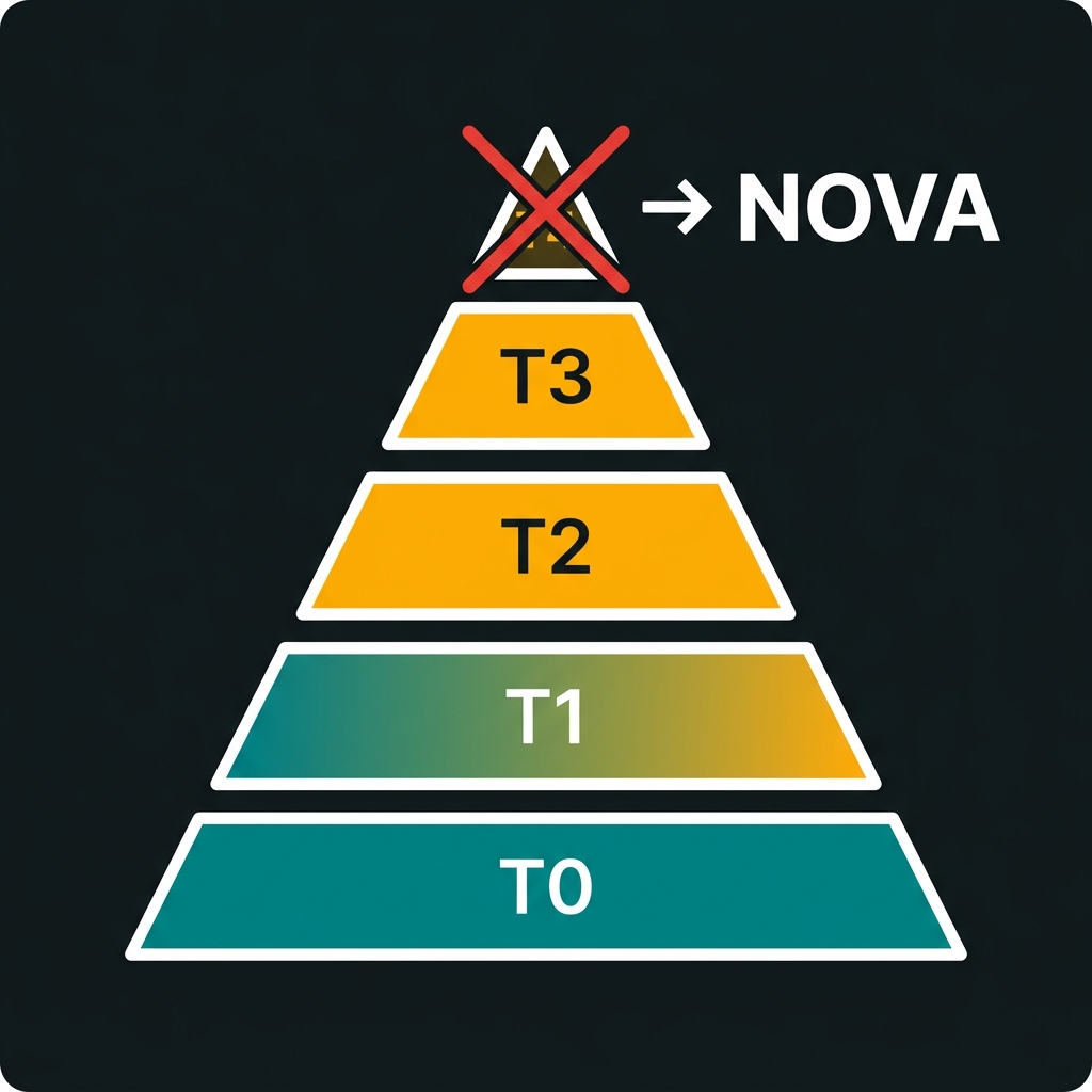
Hybrid symbolic applications
→SOLAR is intermediate decimal-native photonic control — the human-legible control plane between GEMINI qubits and field-native GALAXY/NOVA.
- T0 Bring-up — comb lock cert, confusion matrix, gate tomography
- T1 Control — decimal phase schedules, calibration tables
- T2 Arithmetic lab — SDCLA demo, native DADD/DMUL benchmarks
- T3 Symbolic hybrid — spectral register as visible state machine
- T4 AI / crypto — defer to NOVA (MATMUL10, RS coding)
Hybrid workflow: engineer reads digit 7 on OSA → firmware writes |7⟩ = |1⟩⊗|2⟩ → SDCLA DADD → OPC refresh → demux confirms ch7.
How we do it: Ship SOLAR SDK with decit_write(d), decit_read(), dadd(a,b); bundle calibration suite (C-matrix + PHASE sweep + SDCLA golden tests); publish migration guide to GALAXY for field inverse/DIV needs.
Key diagrams
Engineering blueprint style — teal (band A / 0–4), gold (band B / 5–9), orange (OPC).
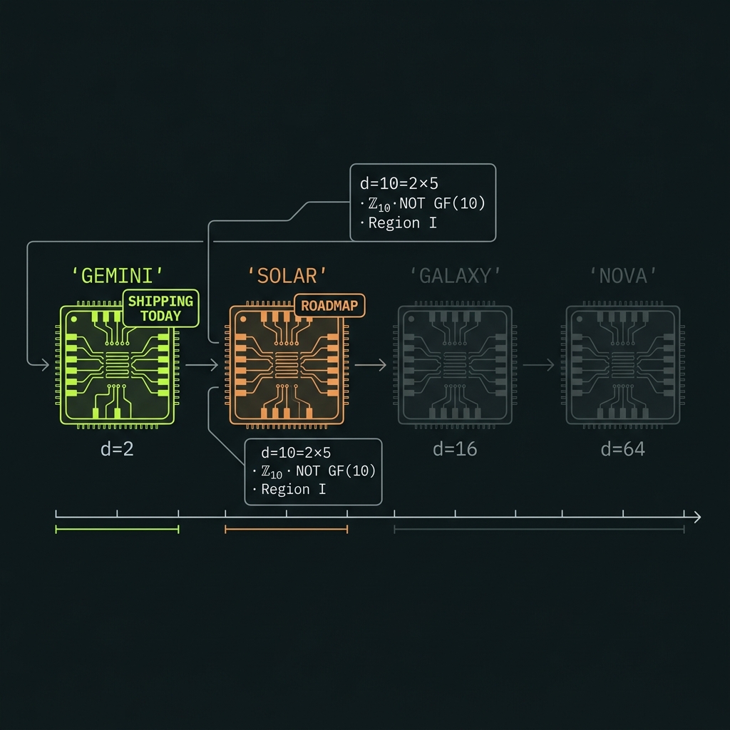 Fig 1
Fig 1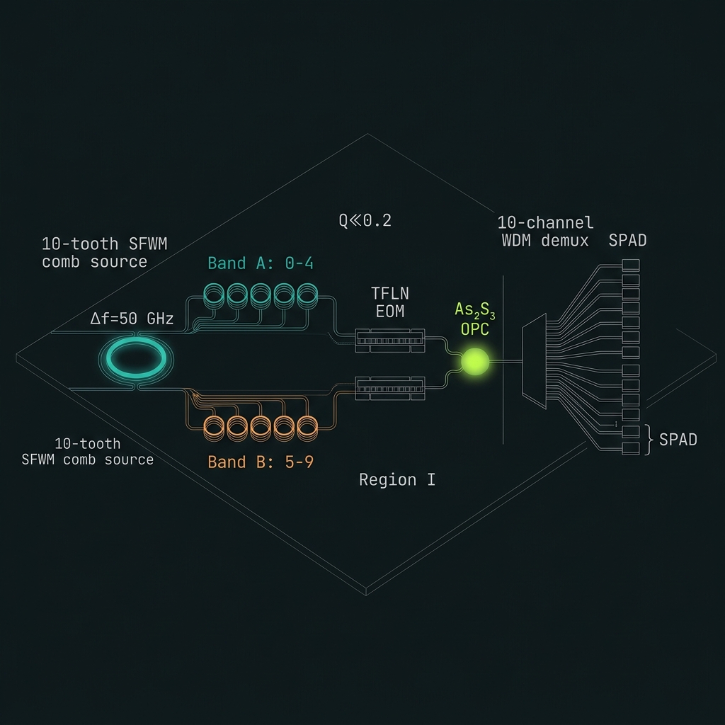 Fig 2
Fig 2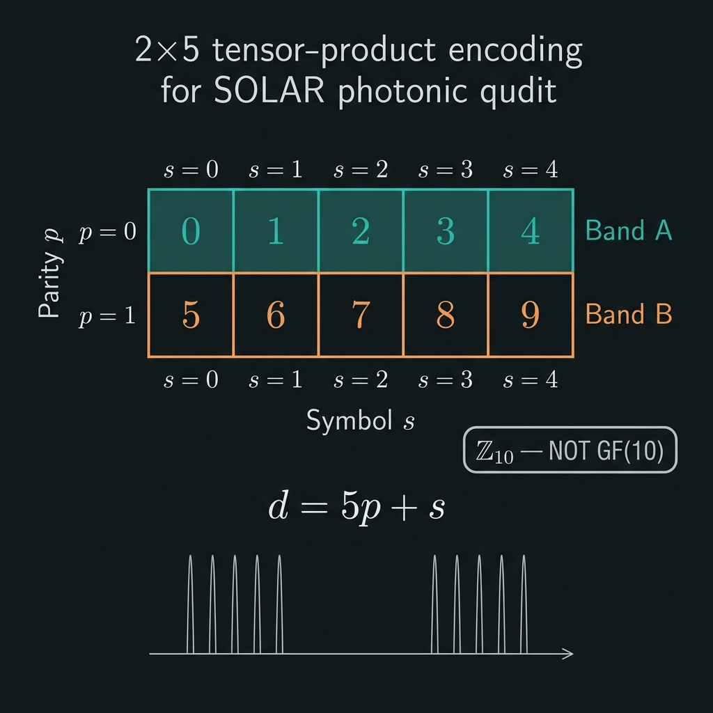 Fig 3
Fig 3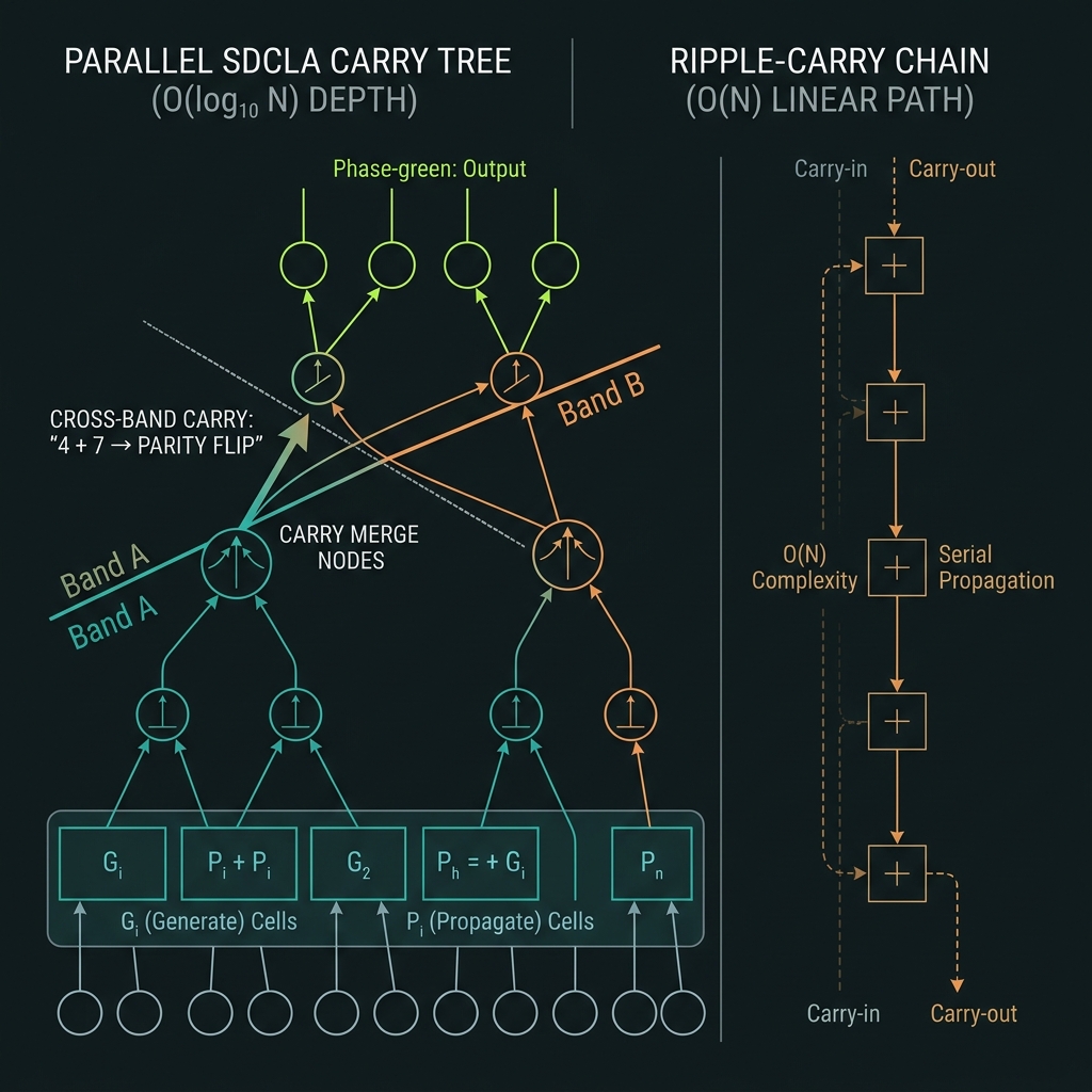 Fig 4
Fig 4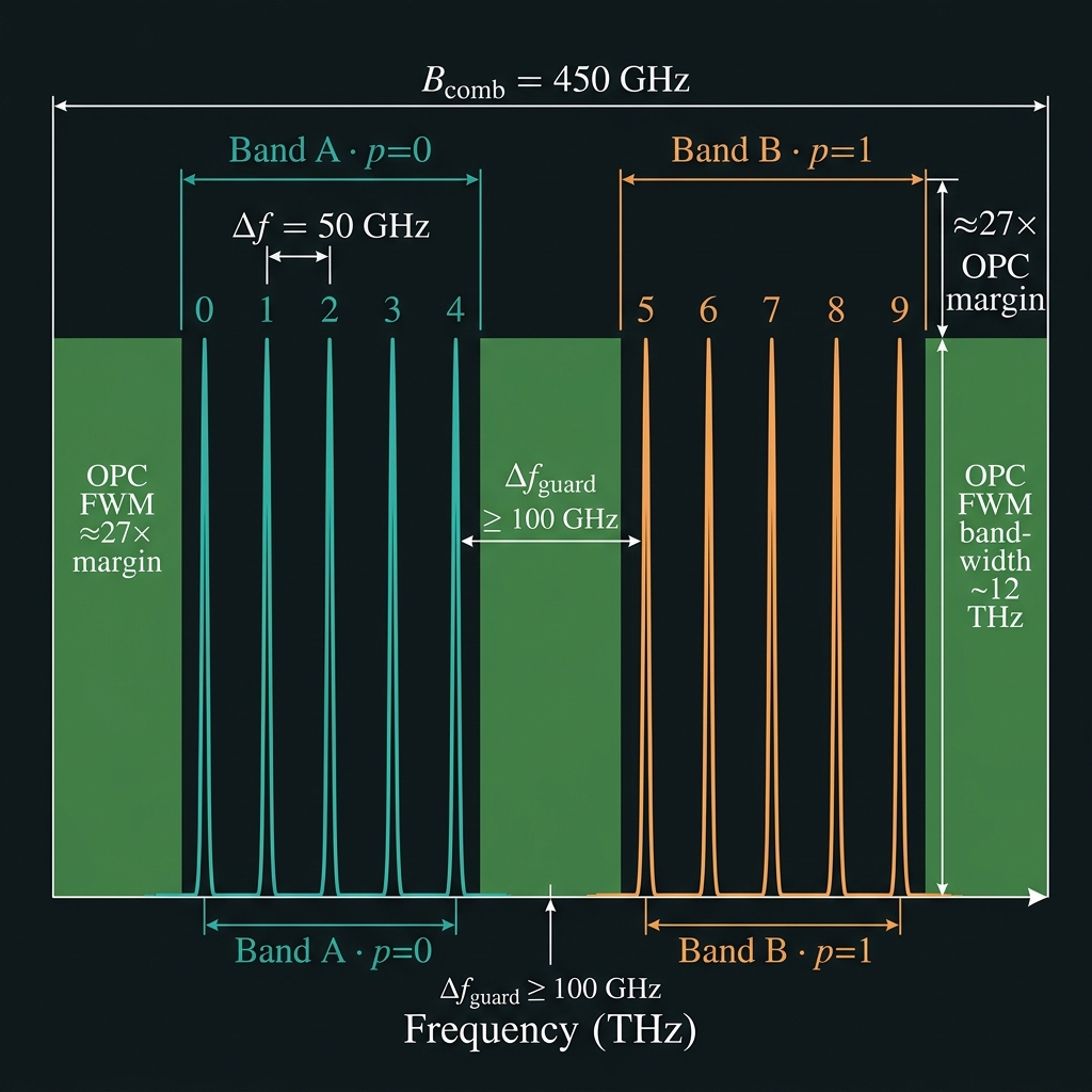 Fig 5
Fig 5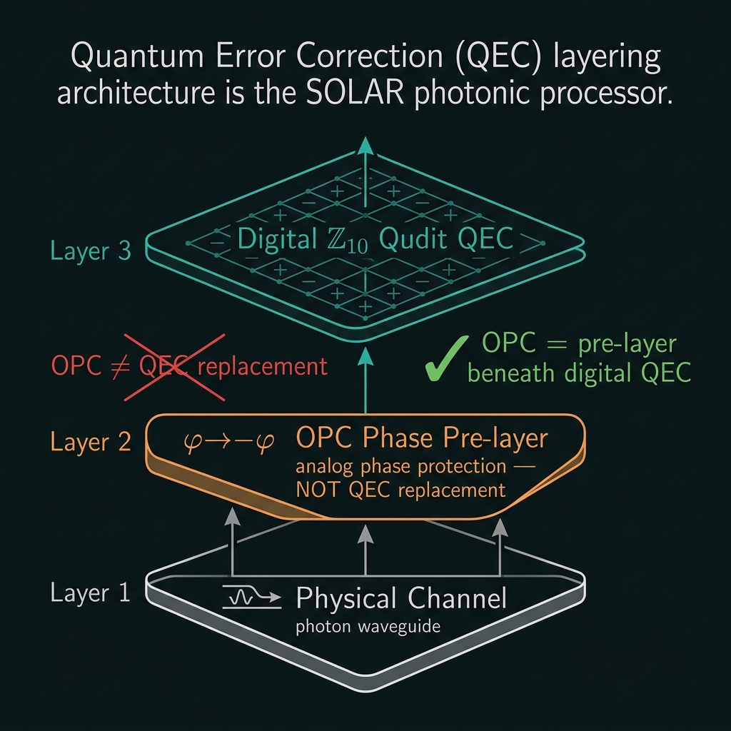 Fig 6
Fig 6Bill of materials + control stack
Every component in the SOLAR system — from silicon nitride to decimal firmware — with vendor part numbers and sourcing.
Foundry never sees arsenic or OPC geometry
Phase A — FEOL: LIGENTEC AN800 MPW. Si₃N₄ comb ring, AWG demux, dual 5-ring shapers, 10-ring WDM routing, 13 heater channels. Encrypted GDS-II, OPC geometry withheld.
Phase B — TFLN bond: QLT internal. Ion-cut LiNbO₃ onto SiN for EOM and QFP cascades.
Phase C — As₂S₃ BEOL: QLT arsenic-isolated cleanroom. 6N-purity chalcogenide thermal evaporation at <210 °C. FWM boundary OPC nodes.
Unique decimal encoding: SOLAR is d=10 — a 2×5 composite, not a prime power. Arithmetic uses ℤ₁₀ (ring with zero divisors), not a Galois field. The 10-tooth comb maps naturally to decimal digit states.
What changes for d=10
10-tooth comb (not 16 or 32) — structured 2×5 composite means ℤ₁₀, not a field. Two 5-ring shaper banks replace the 8-mode Clements mesh.
13 heater channels — simpler thermal control than GALAXY's layout; driven by a single AD5372 (vs. GEMINI's 2×).
OPC margin ~27× — the most headroom of any STAR-PHASER chip. 450 GHz comb span vs. 12 THz OPC bandwidth gives ~27× margin for phase-conjugation fidelity.
AWG demux replaces the Clements MZI mesh; routing is WDM frequency-domain, not spatial-mode interference.
LUV language → QIL middleware → FPGA firmware → photonic chip
The full control stack from user code to decimal photon.
run_freqbin_shot — frequency-bin measurement for d=10 qudit statesDQFP decimal-specific firmware: digit parity, carry-check, ℤ₁₀ syndrome decode
dac.voltages[13] → 13 heater channels → crosstalk-corrected 0–5 V for AD5372grid_valid interlock — comb lock verification before every shot
As₂S₃ OPC FWM boundary nodes · TFLN EOMs · 10-ring WDM routing
From SOLAR roadmap to today's platform
GEMINI ships dual-rail today. The decimal → GF(64) ladder, manufacturing path, and full chip lineup live on sibling pages.