SUPER — Foundry PADP
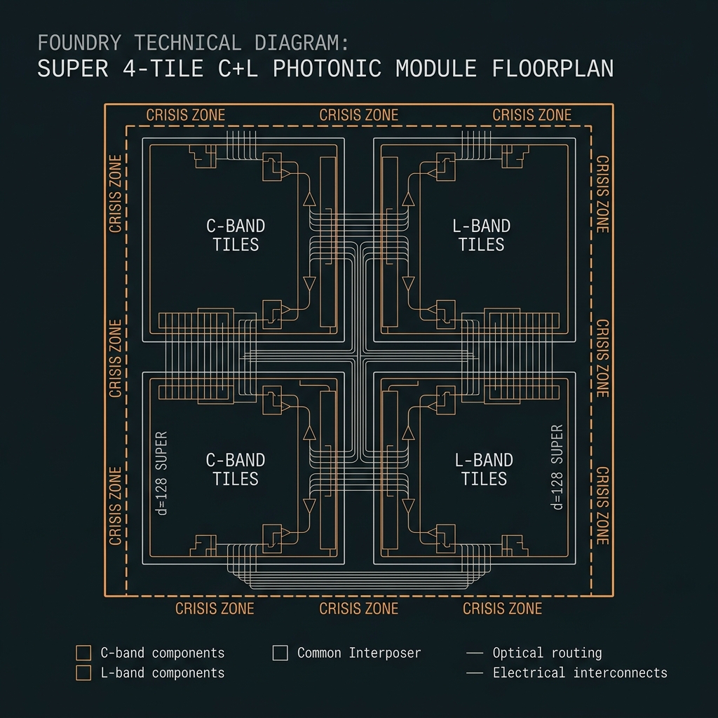
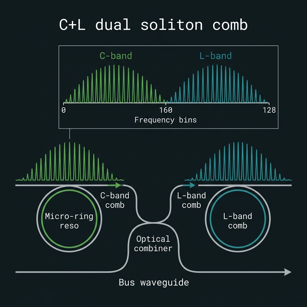
C+L dual-band QUASAR at d=128: 4-tile layout, 35 GHz spacing, seam-lock subsystem, 5-zone TEC, KGD mandatory (FPY ~1–2% without). Roadmap appendix — risk framing, not immediate MPW ask.
Platform summary
4-tile G46 scaled
Tiles: 4
2.5–4 W
Scaled 2.5D interposer
Detection stack
128 SPAD (32× mux) + 16 BHD
 F-U01
F-U01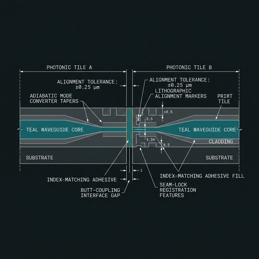 F-U02
F-U02Layer stack & materials
Shared L0–L11 platform across all eight PADPs — Si₃N₄ backbone, TFLN control, As₂S₃ LoCA BEOL (<210°C golden rule), optional AlGaAs MTP.
| Layer | Description |
|---|---|
| 4-tile FEOL | C-band + L-band dual-source tiles |
| Interposer | Scaled 2.5D — seam-lock optical + thermal |
| BEOL | 16–24 LoCA + 14–22 AlGaAs MTP |
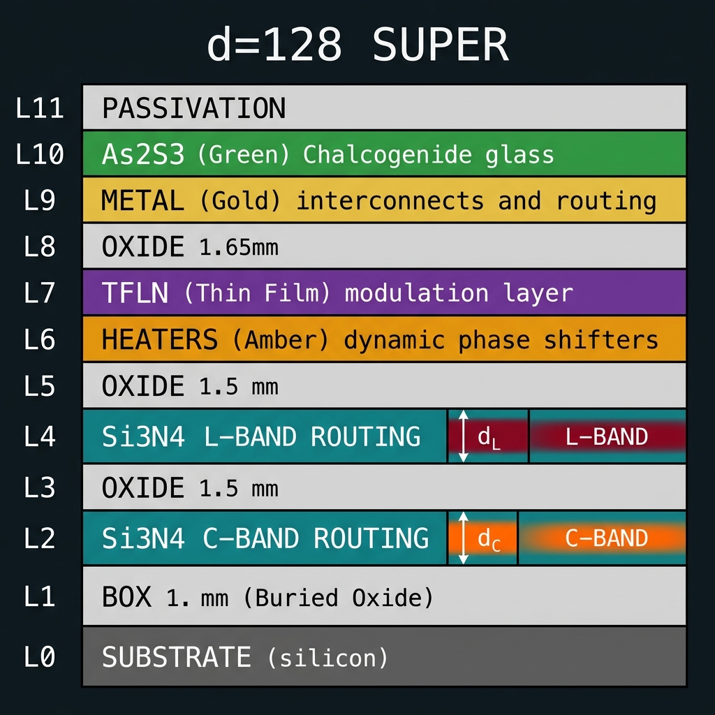 Stack
StackDevice library
On-chip component inventory — status labels per R25 honesty audit.
| Device | Specification | Status |
|---|---|---|
| Dual comb | C+L dual-band source; B_comb ≈ 4.45 THz | designed/target |
| Seam lock | Phase-coherent stitch across 4 tiles | designed/target |
| 5-zone TEC | Independent thermal zones | designed/target |
| Demux 128 | 128-bin readout path | designed/target |
| Holographic readout | Partial holographic mux option | roadmap |
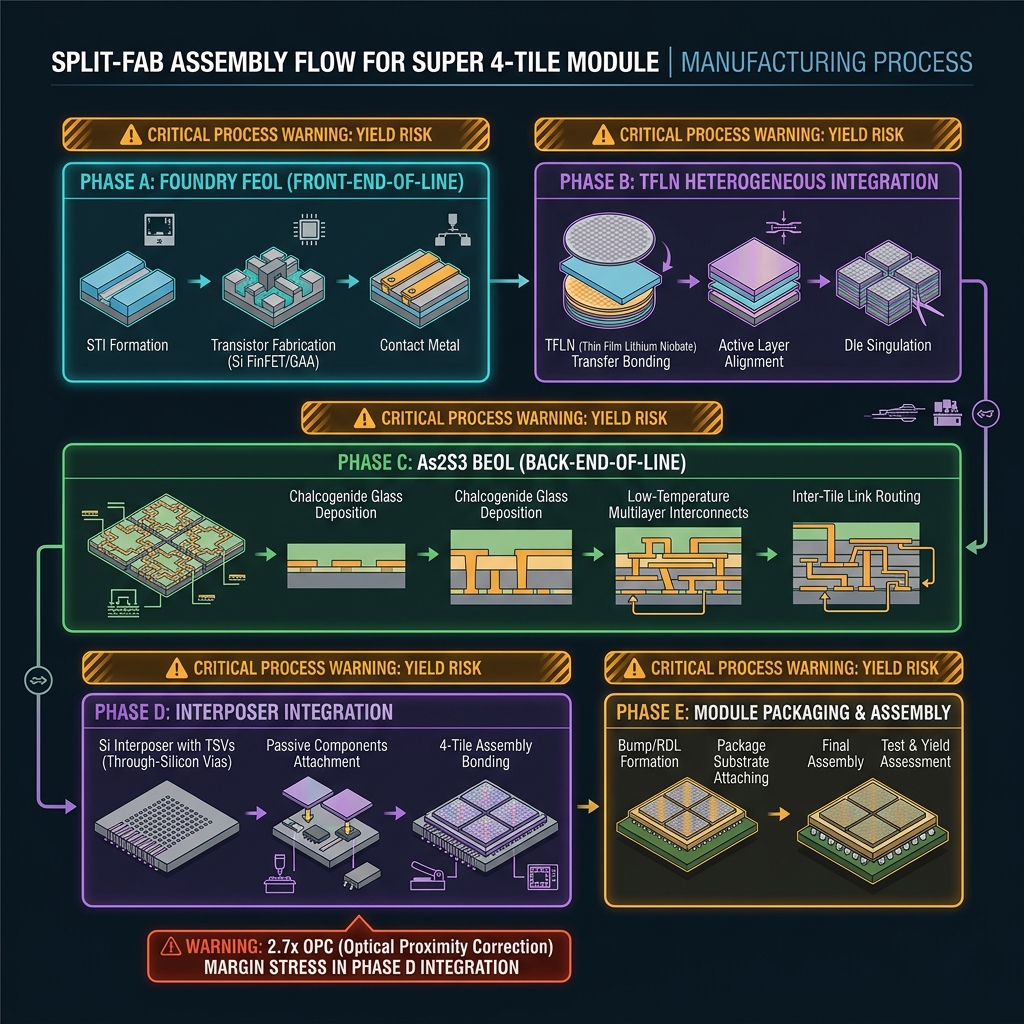
Split-fab phases & assembly
Ligentec FEOL → QLT TFLN bond → arsenic-isolated As₂S₃ BEOL → hermetic package. Foundry never sees arsenic, LN donor recipes, or full OPC geometry.
LIGENTEC AN350
L0–L7 Si₃N₄ FEOL
QC: Gate 0 DRC/LVS/MRC pre-tapeout
→ Planarized wafer or diced dies
QLT bond bay
L8 TFLN ion-cut bond ≤500°C
QC: Gate 1B bond yield + adiabatic IL
→ 18+ EO sites bonded
QLT arsenic BEOL
L9 metal + L10 As₂S₃ <210°C
QC: Gate 2 OPC G≥+2 dB classical
→ Processed dies with LoCA fill
QLT assembly
Dice · fiber · SPAD · seal
QC: Gate 3 packaged acceptance
→ Hermetic module + test report
KGD mandatory — do not assemble untested dies. Seam-lock calibration is critical path. 5-zone TEC co-control firmware on FPGA.
 Assembly
Foundry requirements & intake gates
What the foundry receives vs. what QLT retains. Partial GDS via encrypted transport.
| Item | Requirement / status |
|---|---|
| Posture | Roadmap appendix — co-development orientation only |
| KGD | Mandatory — FPY economics require per-die disposition |
| Risk | Region II high-risk Q ~0.50 — OPC/squeezing co-equal with linear mesh |
| Gates | Seam-lock witness structures on each tile |
Campaign intake gates (all chips)
| Gate | Requirement | Status |
|---|---|---|
| Intake checklist | 00-FOUNDRY-INTAKE-CHECKLIST.md completed per chip/foundry | Open |
| NDA / PDK | DKLA executed; active rule deck downloaded and versioned | Open |
| Gate 0 | Partial-GDS export, DRC/LVS, Q-layer strip audit, SHA-256 hash | Open |
| Wafer probe / KGD | Per-die disposition traveler (mandatory NOVA+) | Open / N/A |
| Package ICD | Fiber, electrical, thermal, mechanical interfaces as drawings | Open |
| ATP / OQC | Acceptance matrix, soak, fiber pull, hermetic/leak tests | Open |
| Foundry acceptance | Module order, waiver list, COA format, quote in writing | Open |
Open items FQ-01–FQ-08 centralized in 00-FOUNDRY-INTAKE-CHECKLIST.md §9. PDK assumption freeze (AN350/AN800 layer integers, LoCA limits, CD/overlay) is a hard hold before GDS upload. Partial-GDS boundary must be DRC-debuggable without releasing withheld As₂S₃/TFLN/AlGaAs/control maps.
Five-volume structure
Full specs in Foundry Chip Docs/SUPER/QLT-SUPER-PADP-Vol-*
| Volume | Title | Research memos |
|---|---|---|
| Vol I | System Architecture | R01–R04 · blocks, encoding, I/O, power/thermal/package |
| Vol II | Physical Architecture | R05–R09 · layer stack, TFLN, LoCA, floorplan, thermal/electrical |
| Vol III | Device Library | R10–R16 · rings, AWG, mesh, couplers, modulators, OPC, detectors |
| Vol IV | Foundry Requirements | R17–R20 · Ligentec/AIM matrix, custom modules, DRC/IP |
| Vol V | Simulation & Tape-Out | R21–R25 · sim plans, GDS roadmap, honesty audit |
Tape-out readiness & honesty audit
U1 demux-128, U2 L-band dual-comb, U3 readout holo — schematic.
No fabricated simulation results are claimed in Vol V — all campaigns status=planned. No GDS beyond v0.1 heritage layouts. No foundry DRC signoff. Promotion path requires closing gates in SUPER-PADP-ROLLUP.md.
 F-U03
F-U03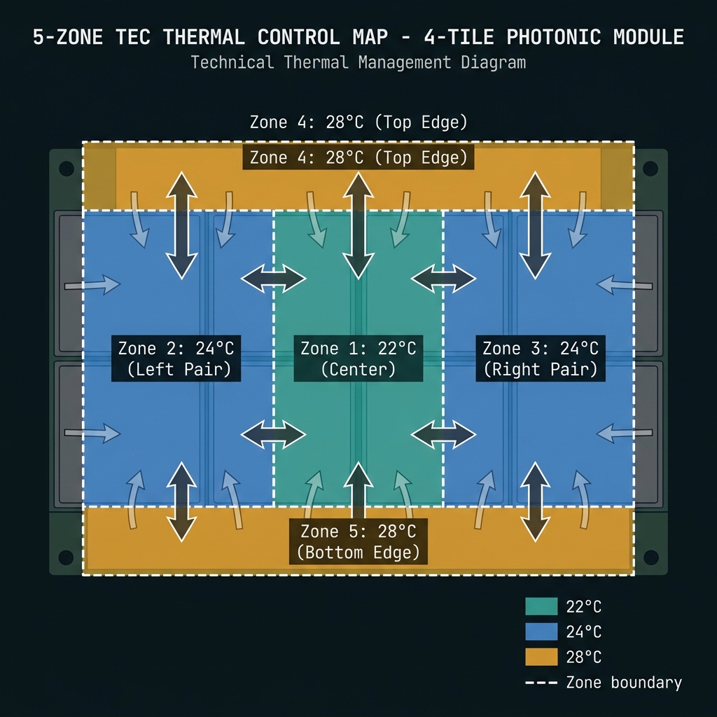 F-U04
F-U04Cross-links
Foundry Chip Docs · Rev B2
On-disk package: Foundry Chip Docs/SUPER/ · Bundle: _export/QLT-PADP-RevB2-2026-06-11.zip