STAR-PHASER GEMINI
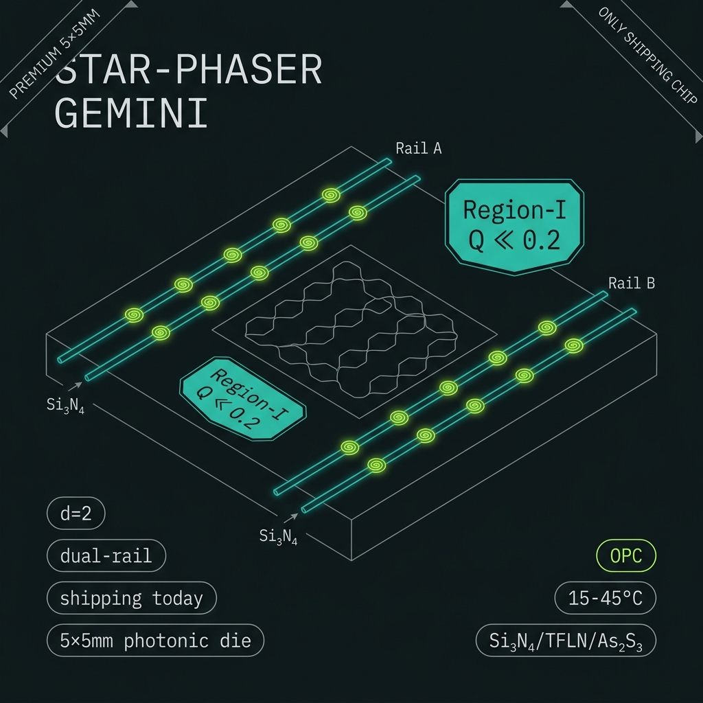
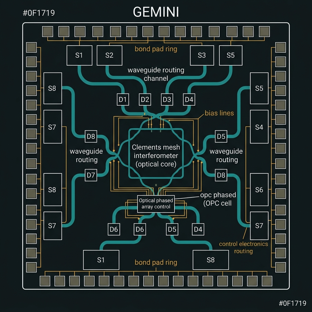
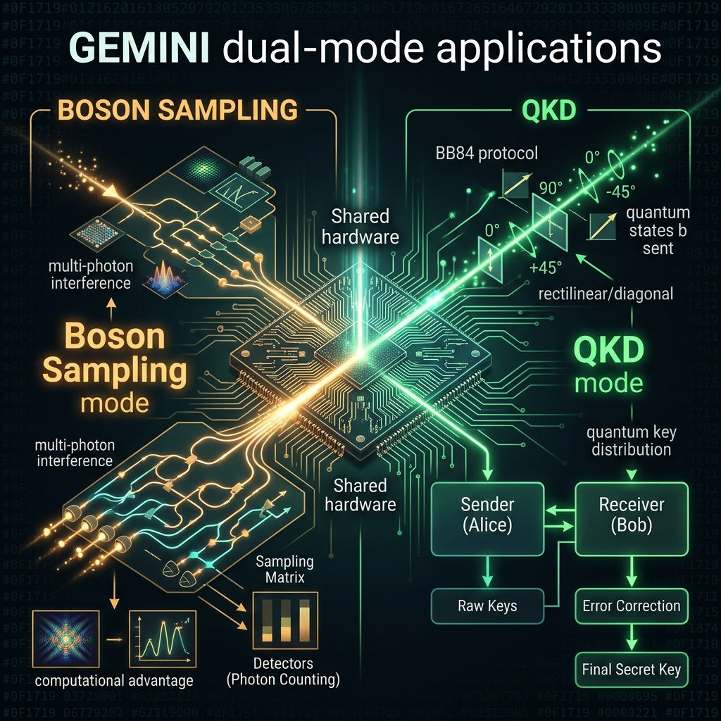
QLT's only shipping STAR-PHASER product today: a room-temperature, dual-rail (d=2) photonic qubit processor in Region I (Q ≪ 0.2), where linear MZI circuits dominate and OPC acts as a passive phase pre-layer beneath digital QEC — not a replacement for it. One photon, two Si₃N₄ waveguides, SU(2) gates on an 8-mode Clements mesh, Type-II fusion entanglement, and warm InGaAs/GeSi SPAD readout at 15–45 °C.
 G-01
G-01GEMINI v1 product parameters
Every value carries a status label. External benchmarks are cited for context — not claimed as QLT measurements unless noted.
| Parameter | GEMINI value | Status |
|---|---|---|
| Brand / codename | STAR-PHASER GEMINI | designed/target |
| Encoding | d=2 dual-rail path · |0⟩ rail A · |1⟩ rail B · 1 bit/photon | designed/target |
| Region / Q-metric | Region I · Q ≪ 0.2 (model ≈ 0.05) | designed/target / model |
| Die footprint | 5 × 5 mm | designed/target |
| Operating temperature | 15–45 °C warm core (mesh, sources, SPAD) | designed/target |
| Wavelength | C-band ~1550 nm | designed/target |
| Gate mesh | 8-mode Clements/Reck · 28 MZIs · 32 thermo-optic heaters | designed/target |
| Switches | 16 (feed-forward + K=8 mux tree) | designed/target |
| Detectors | 16 on-chip SPAD taps; Ge homodyne optional (CV path) | designed/target |
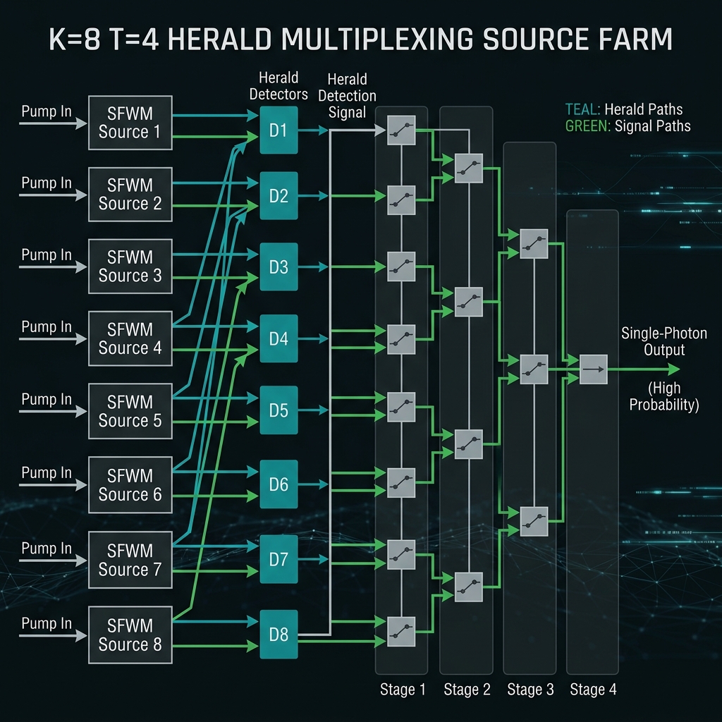
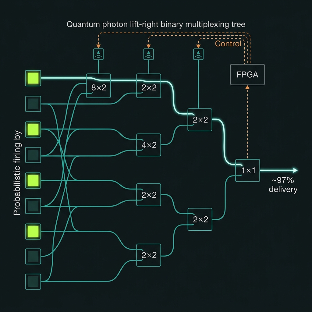
| Sources | K=8 heralded SFWM rings + T=4 temporal slots | designed/target |
| Multiplexed availability | A ≈ 96.6% at p=0.1, K=8, T=4 | model |
| OPC geometry | Recirculating storage loop · M ≈ 10 gates | claim/to-be-tested |
| Gate depth (phase / with OPC) | ~50–100 / 500–1,000+ gates | external limit / designed/target |
| v1 quantum demo | 4-qubit GHZ >85% fidelity | designed/target |
| Dual-use AI mode | Same mesh → photonic AI accelerator (~14 TOPS/W class) | designed/target |
| Δf (frequency-bin) | N/A — path encoding, no comb | designed/target |
| External benchmark (SPAM) | — | PsiQuantum Omega: 99.98% external |
| External benchmark (fusion) | — | PsiQuantum Omega: 99.22% external |
Full platform walkthrough: How We Do ItChips & Mfg OverviewChip Lineup · Roadmap ladder: Base 2 → GF(256) · Chip lineup: STAR-PHASER chips
Eight subsystems on one die
Tap any tile to expand. Each section maps to a WS13 research memo — encoding through applications.
GEMINI stays in Region I: purely linear interferometry between sparse OPC nodes. No frequency-bin routing, no QFP shaper cascades — those belong to SOLAR+ roadmap chips.
GEMINI subsystem stack
Encoding · gates · source · routing · cal · OPC · QEC · appsDual-rail path encoding physics
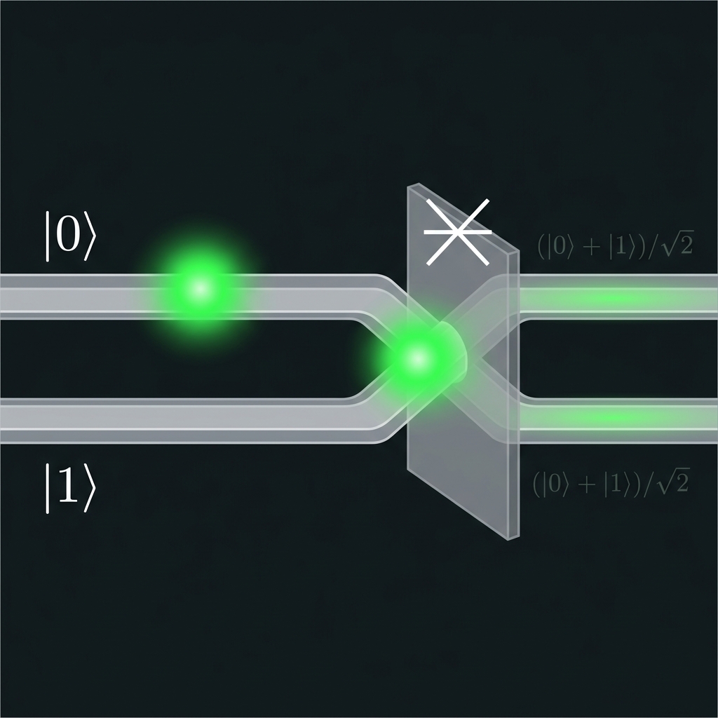
→One qubit = one photon in a two-dimensional path Hilbert space: |ψ⟩ = α|1⟩A|0⟩B + β|0⟩A|1⟩B. Quantum information lives in the amplitude ratio |α/β| (population) and differential phase Δφ = φA − φB (Bloch equator). Global phase φA + φB is unphysical — it cancels in all interferometric readouts.
Loss on one rail without heralding is an erasure — the photon left the {|0⟩,|1⟩} subspace but the defect location is known, which QEC treats more favorably than undetected depolarizing noise. Heralding + coincidence filtering enforce the single-photon subspace at runtime.
d=2 · SU(2) · no spectral crosstalk · no EOM scattering
Upgrade path: optional GAP4 transcode at encoding boundary → 2-color frequency qubit → open comb (d=10, SOLAR roadmap). Native GEMINI computation skips the transcoder entirely.
MZI mesh, SU(2) gates, Type-II fusion
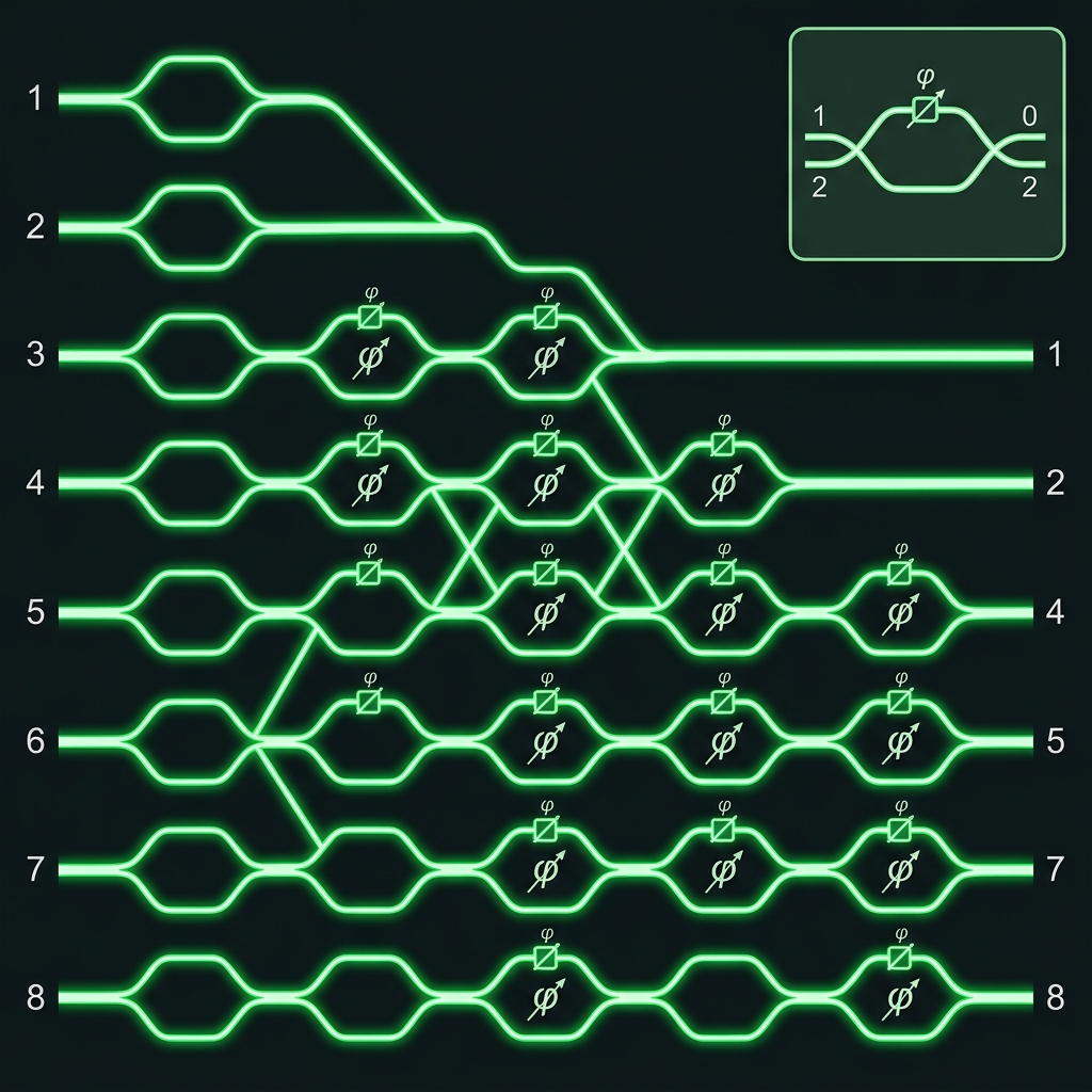
→Single-qubit gates are programs on an 8-mode Clements mesh (28 MZIs, 32 thermo-optic heaters). Arbitrary U(2) per dual-rail pair decomposes into directional couplers (beam splitters) and one-rail phase shifters — Hadamard, Rz, Clifford+T all compile to mesh DAC tables.
Two-qubit entanglement is measurement-based, not deterministic χ⁽³⁾ CZ: Type-II fusion Bell measurements (Psucc = ½ ideal passive LO) + TFLN feed-forward (~11.2 ns budget) steer partner photons in delay spirals. External ceiling: 99.22% fusion fidelity on manufacturable Si (Giewont et al., 2024) — GEMINI targets >99% post-characterization.
Depth without OPC: V(N) = exp(−Nσ²/2) · with OPC every M≈10: V∞ = exp(−Mσ²/2η)
v1 demo: 4-qubit GHZ >85% fidelity on modes 1–8 (four dual-rail pairs).
Heralded SFWM · K=8/T=4 multiplexing
→Eight independent Si₃N₄ micro-rings (R ≈ 50 µm, Q > 5×10⁵) produce heralded pairs via χ⁽³⁾ SFWM at mW-class C-band pumps. Idler clicks flag signal photons; FPGA schedules delivery through a three-stage binary switch tree (7 TFLN EO routers) with T=4 temporal retry slots per source.
Availability law: A = 1 − (1 − p)K·T. At p=0.1, K=8, T=4 → A ≈ 96.6% [model]. Absolute photon-at-output probability PG1 remains switch-loss-limited (~47% [model]) — publish both A and PG1 separately on datasheets.
GEMINI deliberately uses spatial×temporal mux — not Fan 2025 spectral state-multiplexing (roadmap SOLAR path). Δf = N/A on this SKU.
Fab: LIGENTEC AN350-class MPW + proprietary TFLN bond + optional As₂S₃ OPC overlay (~34-week defer-As₂S₃ track available).
Classical switching & interferometric transport
→Two routing regimes on one chip: (1) classical path selection — herald-driven mux tree and feed-forward switches route which mode carries the photon without entangling; success requires low IL, high extinction, phase-stable equalized paths. (2) coherent superposition — MZI mesh routes amplitudes between rails; errors are multiplicative in gate fidelity.
K=8 / 3-stage tree = minimum depth for eight independent herald arms. Per-stage IL target <0.5 dB; extinction >20 dB; path skew ±0.5 µm. Source-stage OPC erases route-dependent phase so muxed photons remain mutually indistinguishable for HOM/fusion.
No 10-ch / 64-ch WDM demux on GEMINI — purely spatial until SOLAR
Technology-agnostic switch socket (P3): TFLN EO committed for mux + feed-forward; thermo-optic for gate mesh; MEMS for lab bring-up only.
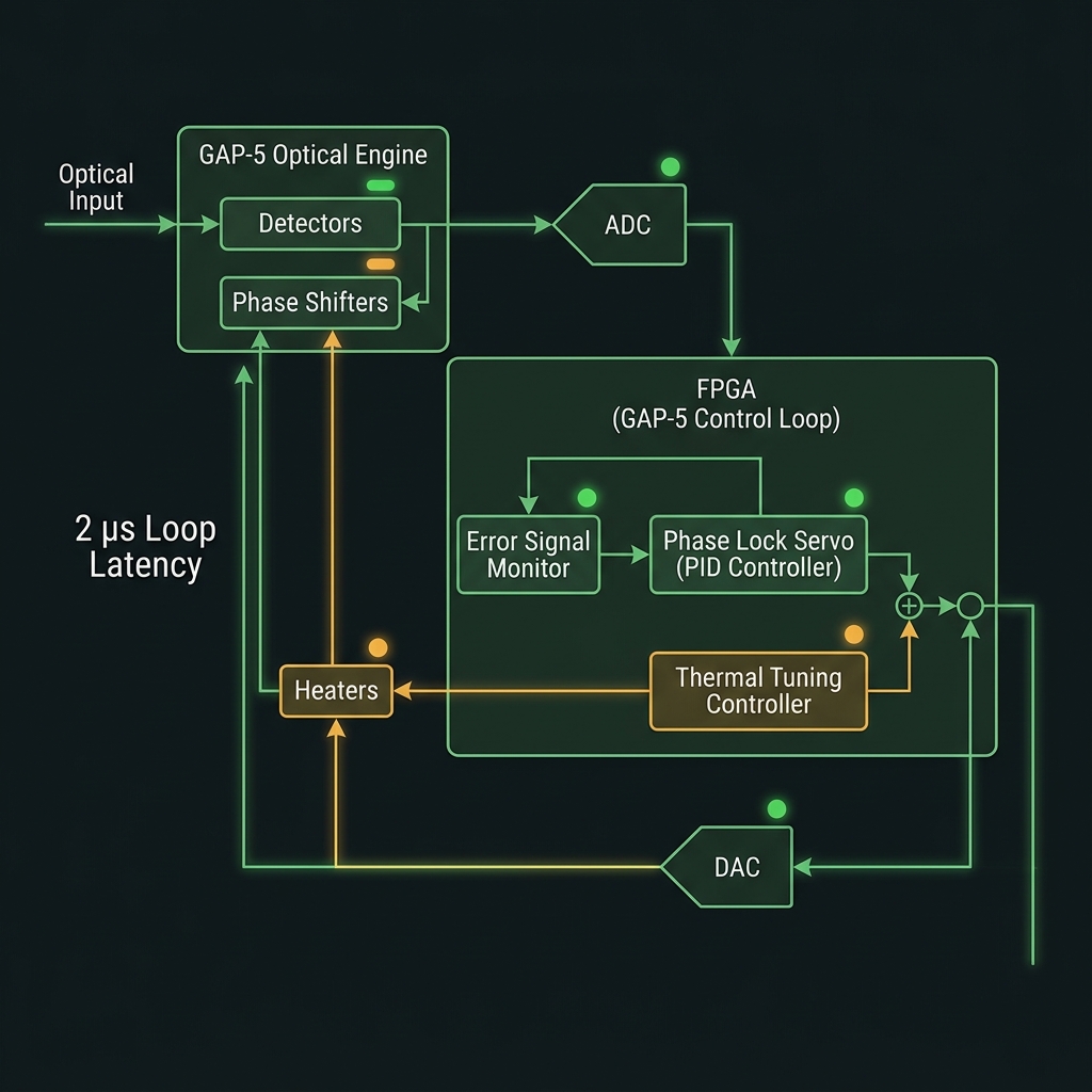
Control stack · GAP5 self-calibration probe
→Control loop: SPAD clicks → 64 ps TDC → FPGA (herald decode, mux select, FF LUT) ↔ AD5372 DAC (32 mesh heaters). Full thermal mesh refresh ~54 µs; feed-forward decision ~11.2 ns (FPGA-limited, switch <2% of budget).
GAP5 OPC visibility probe: V = exp(−σφ²/2) reports differential phase variance from heralded HOM interference — zero added test structures, in-situ during production operation. Drift alarm triggers DAC recalibration when V drops below threshold.
Calibration layers: fabrication trim (once per die) → periodic thermal sweep → mux path equalization (bright-pulse boot) → GAP5 in-situ witness → source_id coincidence validation every shot.
T9 gate: single-photon HOM before/after OPC on dual-rail Sagnac node
OPC lattice · periodic conjugation · baseline CV
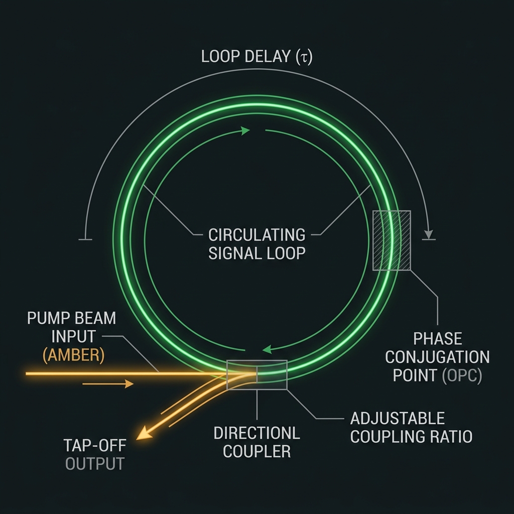
→Hybrid Si₃N₄/As₂S₃ FWM nodes at mux output (GAP2 source-stage) and every M ≈ 10 gates in a recirculating storage loop (GAP1 lattice). Phase conjugation: φ → −φ on each rail; differential encoding lets common-mode pump phase cancel in symmetric layouts.
Without OPC: Var(φ) = N·σ² — visibility collapses ~50–100 gates. With OPC every M gates: V∞ ≤ exp(−Mσ²/2η) — error bounded by interval M and efficiency η, not total depth N.
Optional CV path: Ge p-i-n balanced homodyne @ 15.3 GHz for quadrature readout — baseline CV hardware, not fault-tolerant GKP on shipped SKU. OPC preserves quadrature structure (Gaeta & Boyd, 1995 theory).
Single-photon OPC on-chip: [to-be-tested] · Campaign T9 gates all high-d OPC claims
Never state: OPC replaces QEC — it is an analog phase pre-layer beneath digital stabilizer extraction.
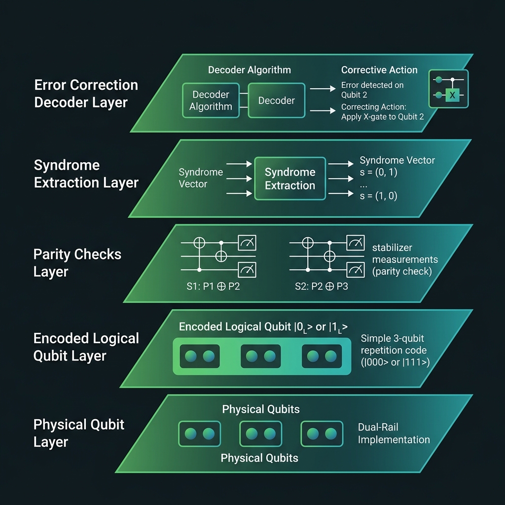
Surface code / stabilizer baseline
→Physical qubit: dual-rail d=2. Stabilizer codes: surface, LDPC, XZZX (bias-aware — OPC Z-preference). Syndrome extraction reuses ancilla MZI programs + per-rail SPAD clicks → FPGA Pauli frame (Path A, v1 ship path).
Industry FT destination (Path B, roadmap): fusion-based quantum computation (FBQC) where resource-state tiles + Type-II fusions encode foliated surface codes — syndromes read from fusion outcomes. GEMINI v1 ships primitives only, not a fault-tolerant fusion network.
Loss maps to heralded erasure (cheap, ~25–50% theory threshold class). Post-OPC model: pZ ~35.7% → ~1.2% at η≥0.5 — moves operating point toward surface-code Pauli threshold (~1%). A507 Stim/PyMatching simulation is software gating.
Logical qubit / break-even QEC: [roadmap] — not GEMINI ship date
Applications · validation · dual-use AI
→Tier A — ship today: dual-rail LOQC processor; photonic AI inference on same 28-MZI mesh (configuration change: pump power, detector mode). Tier B — validation: 4-qubit GHZ >85%, HOM >85%, g²(0)<0.5, CAR >50:1. Tier C — roadmap: decimal/GF compute → SOLAR / NOVA.
Validation hierarchy gates marketing: Layer 1 timing → Layer 2 mesh cal → Layer 3 OPC probe (T9) → Layer 4 fusion+FF → Layer 5 GHZ/algorithms → Layer 6 FBQC factory [roadmap]. Do not skip to Layer 5 claims without Layer 3 evidence when OPC is featured.
External GHZ benchmark: 85.4% integrated Si (2024) — GEMINI >85% target is competitive with integrated photonics SoTA, not bulk telecom or cryo SNSPD platforms.
Customer personas: HPC pilot (no cryoplant), photonic QC research lab, AI/accelerator dual-use, government eval on US-friendly split-fab.
 G-09
G-09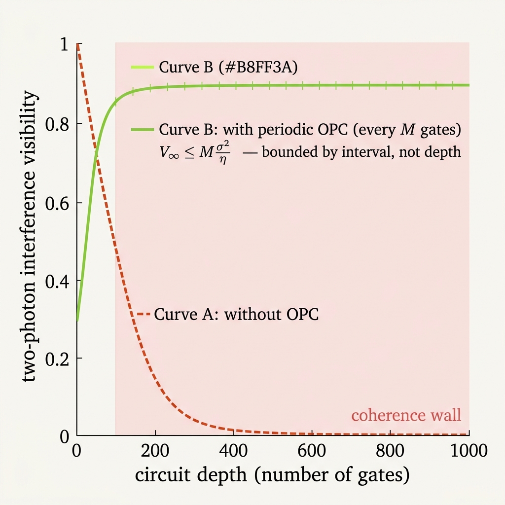 G-15
G-15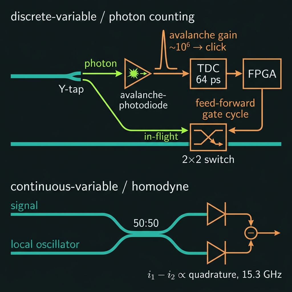 G-08
G-08What goes into GEMINI — and when
Every component that enters the build, organized by manufacturing phase. From foundry wafer to shipping product.
Manufacturing build sequence
FEOL · bond · BEOL · assembly · electronics · softwareSilicon nitride photonic backbone
→Foundry: LIGENTEC AN800 MPW → X-FAB Erfurt 200 mm wafer line. Shuttle LGT-MPW-AN800-44 (registration closes 1 Jul 2026). Backup: AIM Photonics.
Si₃N₄ strip waveguides — 800×400 nm, stoichiometric LPCVD, <0.5 dB/m propagation loss. Forms the entire passive backbone.
8 SFWM microrings — R≈50 µm, Q>5×10⁵, χ⁽³⁾ photon-pair sources. Each ring generates heralded single photons at C-band ~1550 nm.
28-MZI Clements mesh — 8-mode interferometric unitary. Directional couplers + thermo-optic phase shifters implement arbitrary SU(8) gates.
32 TiN thermo-optic heaters — ~54 µs settle time. Driven by AD5372 DAC via SPI. Each heater controls one MZI arm phase.
Feed-forward delay spirals — on-chip optical delay lines matched to the ~11.2 ns SPAD→FPGA→EOM feed-forward loop.
Encrypted GDS-II sent to foundry — OPC geometry withheld. Foundry never sees arsenic or nonlinear overlay.
TFLN electro-optic switch layer
→TFLN thin film — 300–600 nm thin-film lithium niobate, ion-cut bond onto SiN at ≤500 °C. Coupon placement via X-Celeprint micro-transfer printing (MTP).
23 TFLN EO switches — sub-nanosecond switching, >110 GHz bandwidth. 7 multiplexer switches route heralded photons; 16 feed-forward switches implement conditional corrections.
Ti/Au GSG electrodes — 200/500 nm, e-beam evaporation + lift-off. 16 RF ground-signal-ground pads drive the EO switches.
Bond performed in QLT cleanroom — ≤500 °C max, well below As₂S₃ Tg.
As₂S₃ chalcogenide OPC overlay
→As₂S₃ overlay — 6N-purity arsenic trisulfide, 450–550 nm thickness. Thermal evaporation at <210 °C (golden rule: no processing above Tg after deposition). n=2.40, n₂=2–5×10⁻¹⁸ m²/W.
4 FWM-OPC sites — four-wave mixing optical phase conjugation nodes placed every ~10 gates. Recirculating OPC loop geometry enables M≈10 conjugation passes.
MES barcode lockout enforces golden rule — furnace interlock prevents wafer entry above 210 °C.
Packaging, fiber attach, detector bond
→Die: 5×5 mm single tile, diced on DISCO DAD-3220.
Hermetic butterfly package — CVD diamond heat spreader, <0.5 W total dissipation. Kovar-sealed.
Fiber array — SMF-28 (Corning), ExSpot inverse-taper edge coupling. Aligned on PI P-611 NanoCube 6-DOF stage.
SPAD flip-chip bumps — 24 In/Sn bumps (8 herald + 16 mesh), PDE ≥28%. Bonded on SÜSS FC150 at ±1 µm accuracy.
Au wire bonds — 32 heater pads + 16 RF GSG pads, 25–50 µm Au wire via K&S 4523 bonder.
Hermetic seam-seal — final enclosure, leak-tested.
Control hardware, lasers, detectors
→2× Analog Devices AD5372 Rev. C — 32-channel 16-bit DAC, SPI @ 50 MHz, 0–5 V output, LDAC-synchronized. 64 total channels drive 32 TiN heaters with ~54 µs full mesh refresh.
FPGA (prototype): AMD/Xilinx Artix-7 XC7A100T on Digilent Arty A7-100T dev board — 101k logic cells. Herald engine, DAC SPI master, TDC decode.
FPGA (production): AMD/Xilinx Kintex-7 XC7K325T on AMD KC705 — 326k cells, FMC DAC daughter-card, GTX transceivers. Toolchain: AMD Vivado, Verilog/SystemVerilog, XDC timing constraints.
Supervisor MCU: STMicro STM32H7 Cortex-M7 — housekeeping, DFU firmware update, calibration storage, USB-C / UART / I²C interfaces.
Custom 16-ch TDC ASIC — 64 ps time bins, 33-bit words (channel + 16-bit coarse + 9-bit fine), LVDS output to FPGA.
CW pump laser: Santec TSL-570 — 1550 nm, 150 mW, PM fiber output. Drives SFWM photon-pair generation.
Mode-locked clock: Menlo Systems C-fiber — 100 MHz rep rate, 150 fs pulses, 16 control fibres. Provides optical clock for feed-forward timing.
SPAD module: Aurea Technology 12-ch gated InGaAs (primary) — 1550 nm, PDE ≥30%, DCR <2 kHz, gate 1–10 ns. Parallel eval: ID Quantique 12-ch. Backup: MPD PDM-IR.
Compiler → middleware → firmware integration
→LUV Language v0.3 — user writes .luv source → luvc build → QIL IR 0.1.0 bundle. Commands: luvc check, luvc build, luvc run, luvc fmt.
QIL Middleware — three artifact contract: dac.voltages[32] (28 Clements phases → crosstalk-corrected 0–5 V for AD5372), qfp_schedule[] (ordered unitary steps), shot_contract (SPAD herald pattern).
FPGA firmware — herald engine, DAC SPI master (2× AD5372), TDC decode, BRAM LUT, feed-forward loop. 200 MHz clock domain. AMD Vivado toolchain.
Three timing tiers:
Feedforward ~11.2 ns — when after measure → Aurea SPAD → TDC → FPGA BRAM → Menlo trigger → TFLN EO switch
Reconfiguration ~54 µs — mesh, phases → FPGA SPI → 2× AD5372 DAC → 32 TiN heaters
Environment <30 s – 16 min — comb_lock.grid_valid → TEC loop → band heaters → per-tooth servo
From GEMINI to the full platform
GEMINI is the shipping anchor. Explore the photon journey, roadmap ladder, sibling chips, and manufacturing path.
How We Do It
Complete walkthrough of heralded SFWM, OPC lattice, MZI mesh, detection, and feed-forward — the shared backbone GEMINI configures for minimum nonlinear budget (Region I).
Base 2 → GF(256)
GEMINI is Rung 0 (dual-rail, ships). SOLAR opens the comb to d=10; GALAXY–NOVA climb to GF(64) field coding — all proposal-grade beyond GEMINI.
STAR-PHASER & QUASAR lineup
Eight gate-locked chip pages from GEMINI (d=2, ships) through LOTUS (d=512, Region IV). Only GEMINI is solid today; all others ghosted roadmap.