SOLAR — Foundry PADP
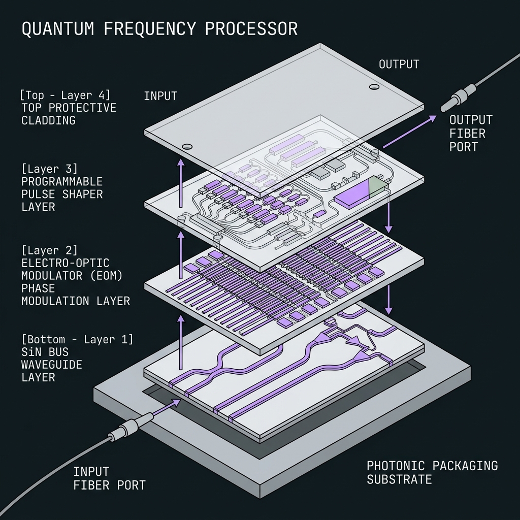
Frequency-bin decit (d=10) roadmap PADP: 50 GHz comb spacing, QFP gate layer (TFLN EOM + microring shaper), AWG demux, and dedicated testchip for comb/dispersion/AWG de-risk. Same split-fab backbone as GEMINI.
Platform summary
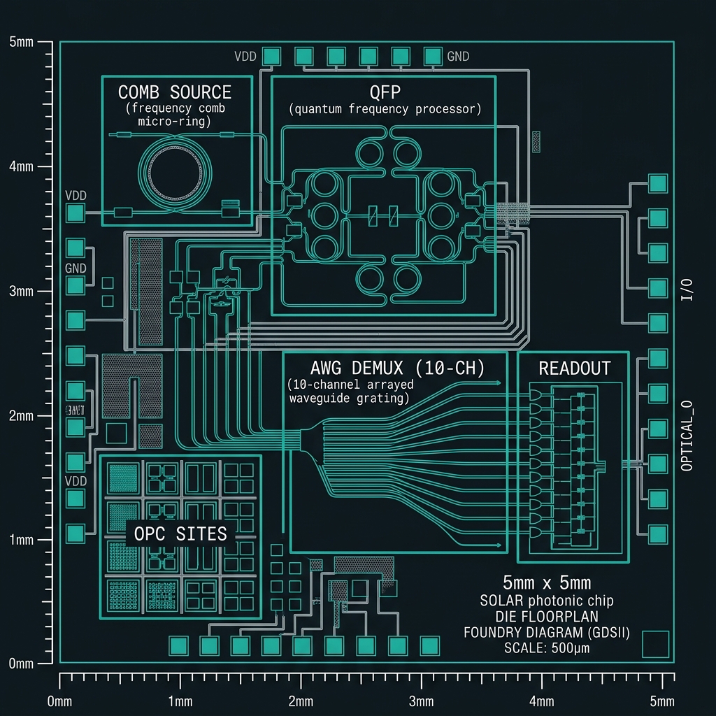
5 × 5 mm + testchip GDS
Tiles: 1
< 0.8 W
24-pin flatpack
Detection stack
10-ch SPAD array + QFP demux
 F-S01
F-S01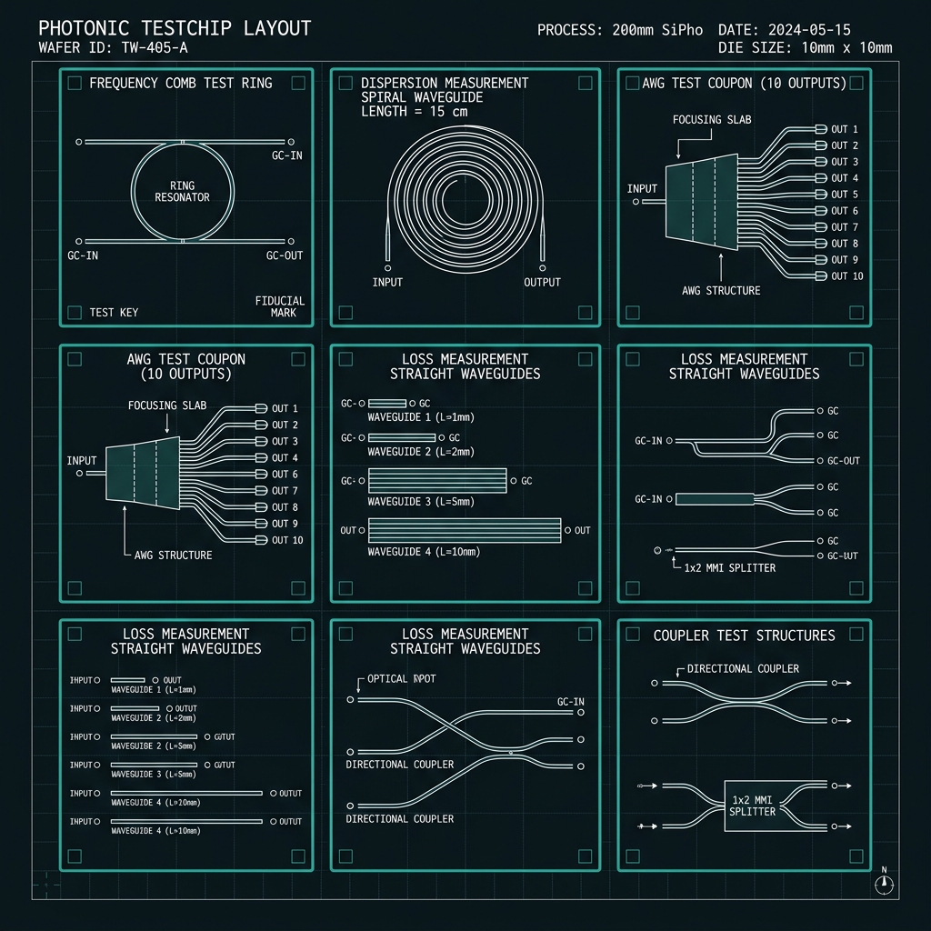 F-S02
F-S02Layer stack & materials
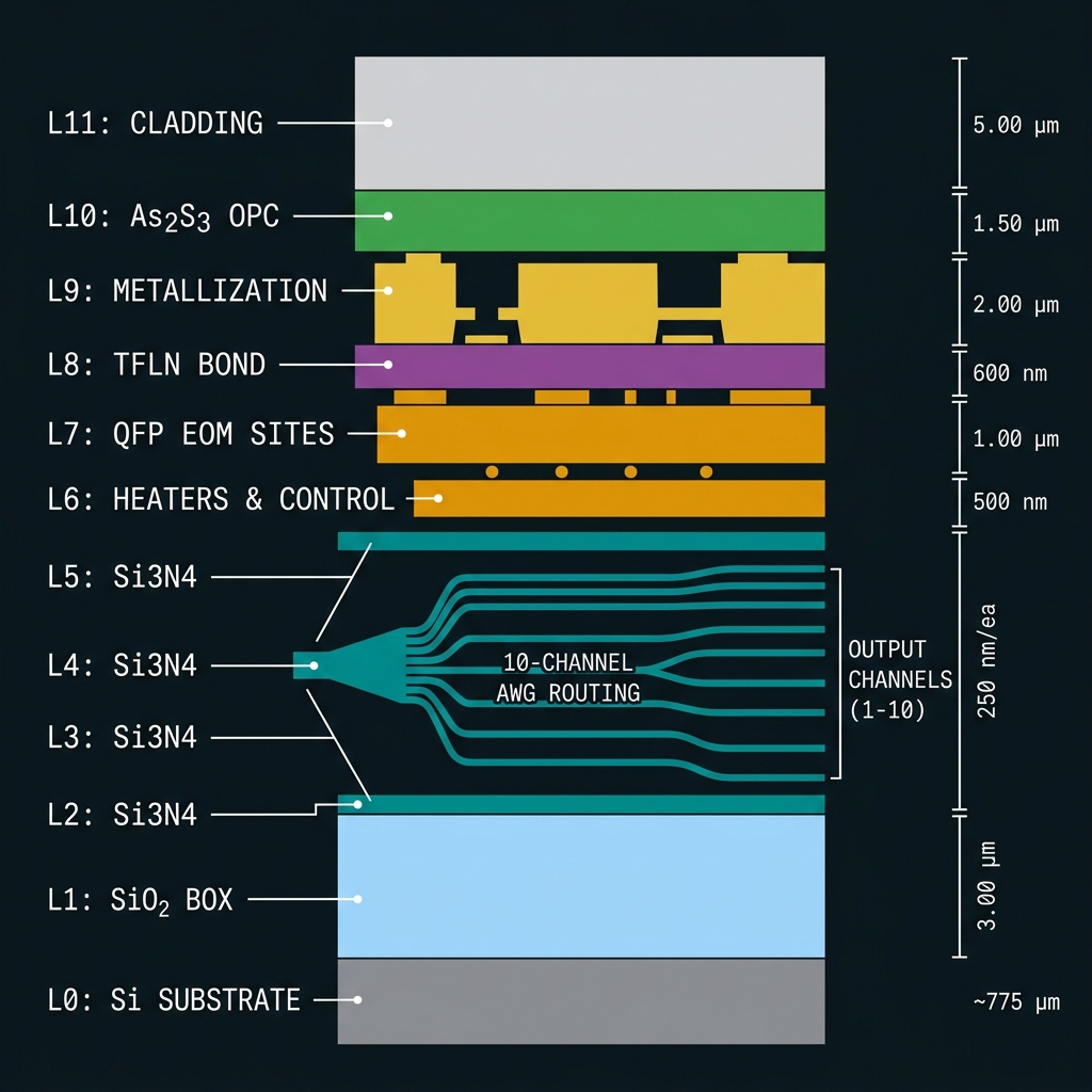
Shared L0–L11 platform across all eight PADPs — Si₃N₄ backbone, TFLN control, As₂S₃ LoCA BEOL (<210°C golden rule), optional AlGaAs MTP.
| Layer | Description |
|---|---|
| L0–L7 | AN350 SiN FEOL — larger ring bank for 50 GHz FSR comb source |
| L8 | TFLN bond — bin-mixer EOMs @ f_RF = Δf |
| L9–L10 | Line-by-line shaper rings + optional As₂S₃ OPC overlay |
| Testchip | Separate GDS: comb, dispersion, loss ladder, AWG coupon structures |
 Stack
StackDevice library
On-chip component inventory — status labels per R25 honesty audit.
| Device | Specification | Status |
|---|---|---|
| Comb source | SFWM / LLE soliton microcomb; 50 GHz spacing; B_comb ≈ 450 GHz | roadmap |
| QFP processor | EOM + Fourier shaper cascade; X₁₀/Z₁₀/F₁₀ generators | designed/target |
| AWG demux | 10-ch 100 GHz grid; −16 to −20 dB crosstalk target | designed |
| OPC module | Broadband single-pass conjugates all 10 bins (>12 THz band) | claim |
| MZI mesh | Reduced vs GEMINI — frequency-domain gates primary | roadmap |
| Detectors | 10 warm SPADs or serial SNSPD + QFP scan | designed/target |
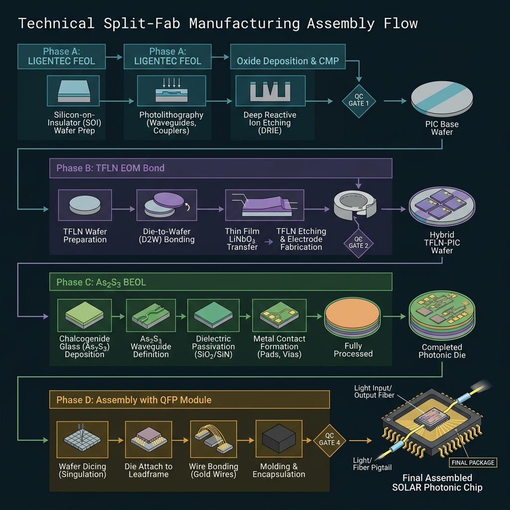
Split-fab phases & assembly
Ligentec FEOL → QLT TFLN bond → arsenic-isolated As₂S₃ BEOL → hermetic package. Foundry never sees arsenic, LN donor recipes, or full OPC geometry.
LIGENTEC AN350
L0–L7 Si₃N₄ FEOL
QC: Gate 0 DRC/LVS/MRC pre-tapeout
→ Planarized wafer or diced dies
QLT bond bay
L8 TFLN ion-cut bond ≤500°C
QC: Gate 1B bond yield + adiabatic IL
→ 18+ EO sites bonded
QLT arsenic BEOL
L9 metal + L10 As₂S₃ <210°C
QC: Gate 2 OPC G≥+2 dB classical
→ Processed dies with LoCA fill
QLT assembly
Dice · fiber · SPAD · seal
QC: Gate 3 packaged acceptance
→ Hermetic module + test report
TFLN wafer-scale bond sub-flow (He⁺ ion-cut) or µTP coupons. Testchip lot can run in parallel on same MPW reticle for comb/AWG characterization before full decit integration.
 Assembly
Foundry requirements & intake gates
What the foundry receives vs. what QLT retains. Partial GDS via encrypted transport.
| Item | Requirement / status |
|---|---|
| Primary | LIGENTEC AN350 + dedicated testchip shuttle |
| Custom modules | TFLN EOM bond; microring shaper bank; AWG mask layer |
| GDS | Main die + QLT-SOLAR-testchip-v0p1.gds |
| DRC | Same campaign dry-run posture as GEMINI — Open |
| Gates | T-B07 demux/QFP characterization gates before decit claim |
Campaign intake gates (all chips)
| Gate | Requirement | Status |
|---|---|---|
| Intake checklist | 00-FOUNDRY-INTAKE-CHECKLIST.md completed per chip/foundry | Open |
| NDA / PDK | DKLA executed; active rule deck downloaded and versioned | Open |
| Gate 0 | Partial-GDS export, DRC/LVS, Q-layer strip audit, SHA-256 hash | Open |
| Wafer probe / KGD | Per-die disposition traveler (mandatory NOVA+) | Open / N/A |
| Package ICD | Fiber, electrical, thermal, mechanical interfaces as drawings | Open |
| ATP / OQC | Acceptance matrix, soak, fiber pull, hermetic/leak tests | Open |
| Foundry acceptance | Module order, waiver list, COA format, quote in writing | Open |
Open items FQ-01–FQ-08 centralized in 00-FOUNDRY-INTAKE-CHECKLIST.md §9. PDK assumption freeze (AN350/AN800 layer integers, LoCA limits, CD/overlay) is a hard hold before GDS upload. Partial-GDS boundary must be DRC-debuggable without releasing withheld As₂S₃/TFLN/AlGaAs/control maps.
Five-volume structure
Full specs in Foundry Chip Docs/SOLAR/QLT-SOLAR-PADP-Vol-*
| Volume | Title | Research memos |
|---|---|---|
| Vol I | System Architecture | R01–R04 · blocks, encoding, I/O, power/thermal/package |
| Vol II | Physical Architecture | R05–R09 · layer stack, TFLN, LoCA, floorplan, thermal/electrical |
| Vol III | Device Library | R10–R16 · rings, AWG, mesh, couplers, modulators, OPC, detectors |
| Vol IV | Foundry Requirements | R17–R20 · Ligentec/AIM matrix, custom modules, DRC/IP |
| Vol V | Simulation & Tape-Out | R21–R25 · sim plans, GDS roadmap, honesty audit |
Tape-out readiness & honesty audit
S1–S3 encoder fidelity, C2 LLE comb, AWG transfer plots — schematic tier. Vol V honesty: no silicon results.
No fabricated simulation results are claimed in Vol V — all campaigns status=planned. No GDS beyond v0.1 heritage layouts. No foundry DRC signoff. Promotion path requires closing gates in SOLAR-PADP-ROLLUP.md.
 F-S03
F-S03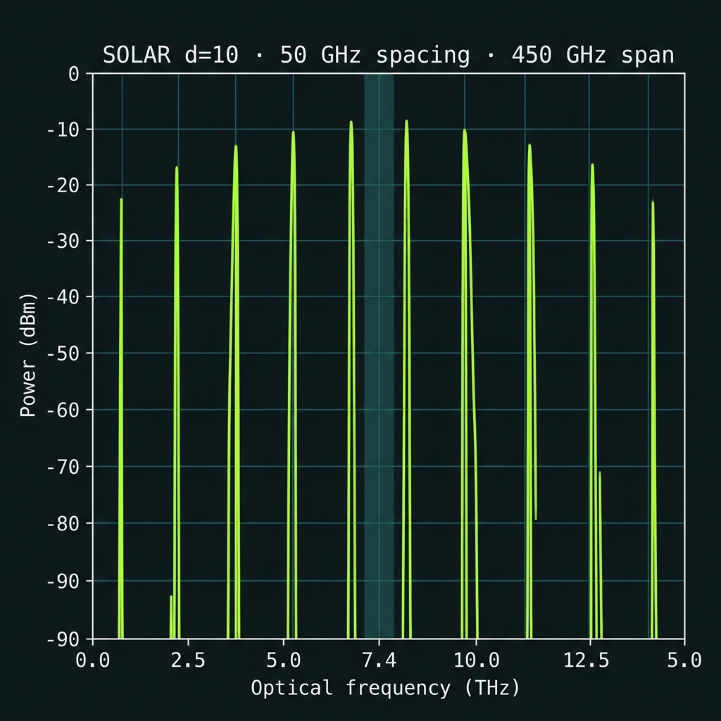 F-S04
F-S04Cross-links
Foundry Chip Docs · Rev B2
On-disk package: Foundry Chip Docs/SOLAR/ · Bundle: _export/QLT-PADP-RevB2-2026-06-11.zip