TETRIS
Transdimensional Encoding Test for Region-I Interferometric Spectral control
STAR-PHASER · d=32 · GF(2⁵) · Last pure STAR-PHASER
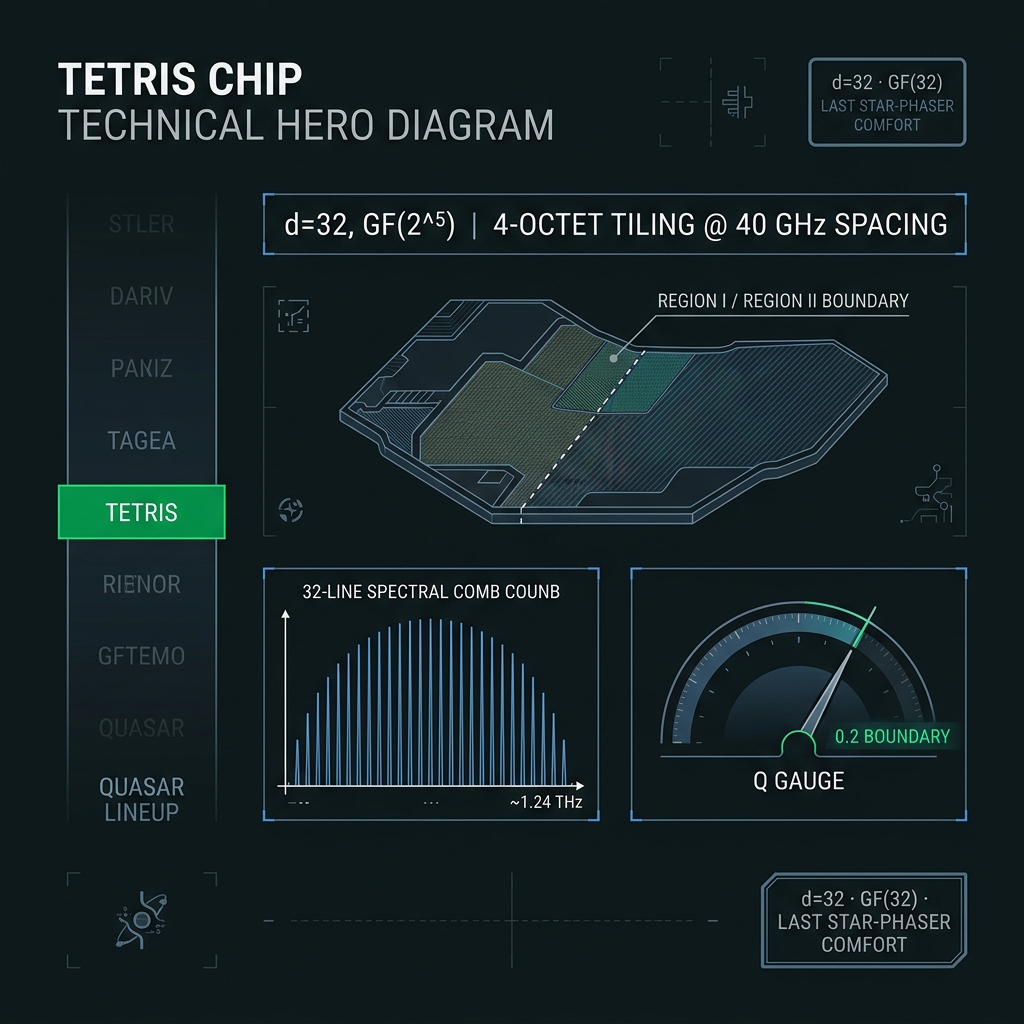
TETRIS is the final gate-locked product in Region I (Q < 0.2) before the lineup crosses into QUASAR NOVA (d=64, Region II). One photon, thirty-two spectral colors, 5 bits/photon, native GF(32) = GF(2⁵) algebraic control — a deliberate scaling stress test, not a shipping v1 SKU.
From TETRIS upward, AWG spectral resolution and adjacent-channel crosstalk — not OPC bandwidth — become the first fab-limited routing ceiling. OPC remains broadband (>12 THz); Hilbert dimension stays comfortable at d=32. Spectral routing fidelity does not.
TETRIS specification ledger
Canonical numbers from WS13 Δf table and S31–S40 corpus.
Q = (H_NL + H_OPC + H_CV) / H_linear

Region I (STAR-PHASER):  Q < 0.2   ← TETRIS lives here
Region II (QUASAR):      0.2 – 1     ← NOVA begins

TETRIS: last chip where OPC is a
periodic weak perturbation beneath
digital QEC — not a field-computing layer.
Lineage: GEMINI (d=2) → SOLAR (d=10) → GALAXY (d=16) → TETRIS (d=32) → Region boundary → NOVA (d=64, QUASAR).
| Property | Value | Status |
|---|---|---|
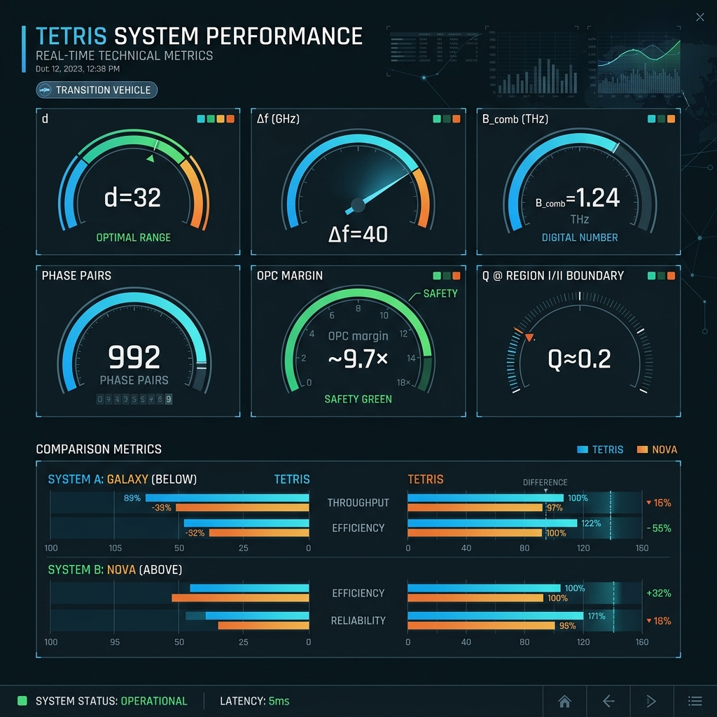
| Hilbert dimension d | 32 = 2⁵ | roadmap |
| Algebraic layer | GF(32) = GF(2⁵), char 2 | roadmap |
| Bits / photon | 5 | info-theoretic |
| Comb spacing Δf | 50 GHz | designed/target |
| Comb span Bcomb | ≈1.55 THz (31×Δf) | model |
| OPC bandwidth margin | ≫12 THz (~8× headroom) | claim |
| Phase relationships | N(N−1) = 992 | model |
| FWM pathways | ~32k (d²(d−1)) | model |
| QFP cells (~Reck) | ~496 | model |
| First fab limit (TETRIS↑) | AWG resolution / crosstalk | flagged |
| STAR-PHASER purity | Last Region I linear chip | strategic |
 T-01 · Hero
Scaling stress test thesis
S31 — why TETRIS exists on the encoding ladder.
Three hypotheses, one die
Field arithmetic · OPC one-pass · Fab stops before physics5-bit field arithmetic on QFP mesh
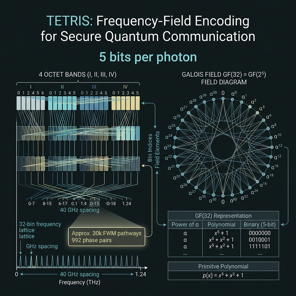
→GF(32) log/antilog multiply, XOR-add, and RS(31,·) syndrome extraction remain tractable on the quantum frequency processor mesh. Primitive polynomial p(x) = x⁵ + x² + 1 committed globally; bin k labeled α^k.
How we do it: 5-bit symbol registers for GFADD/GFMUL kernels alongside SU(32) QFP cascade (S33).
OPC still one-pass at 1.55 THz
→1.55 THz comb span ≪ 12 THz FWM acceptance — conjugation should remain bin-uniform if pump power and β₂ engineering scale. Relative spectral encoding preserves inter-bin phase relationships across all 32 lines.
How we do it: Hybrid Si₃N₄/As₂S₃ OPC nodes every M=10 gates; comb-derived multi-pump refresh (G45).
Fab stops before physics
→32-channel AWG demux, comb lock, and crosstalk isolation fail before OPC bandwidth or Hilbert dimension. TETRIS asks explicitly: can we jump GALAXY→NOVA, or is the 32-ch AWG de-risk necessary?
Campaign flag: AWG resolution gates scale from TETRIS upward
 T-02 · Dashboard
Dense frequency packing at d=32
S32 — 32-dimensional frequency-bin Hilbert space and GF(32) labeling.
Single-photon qudit state: |ψ⟩ = Σk=031 ck|fk⟩ with Σ|ck|² = 1. Bins separated by Δf = 50 GHz; comb spans Bcomb ≈ 1.55 THz centered near 1550 nm.
p(x) = x⁵ + x² + 1   (primitive over GF(2))
GF(32) ≅ GF(2)[x]/(p(x))
|f_k⟩ ↔ α^k   for k = 0…31

Pathways ≈ d²(d−1) = 32² × 31 ≈ 31,744 ≈ 32k
Critical honesty: Bin index k is not integer addition in GF(32). Gates implementing X₃₂ are SU(32) permutations, not field addition.
At d=32, filter skirt overlap between bins k and k±1 becomes non-negligible if AWG 3-dB bandwidth exceeds ~40 GHz — directly tying encoding physics to AWG resolution.
| Δf | 50 GHz (recommended) |
| Per-bin δf (EOM) | ~5–10 GHz FWHM |
| Guard ratio Δf/δf | ≈5–10× |
| Raman null | ~7.4 THz detuning (~15 bins) |
How we do it: Phase-locked 32-line comb; mask-programmed k → 5-bit polynomial ROM; EOM spectral shaping; 32-ch AWG drop filters with crosstalk < −20 dB target; OPC boundary preserves relative phases; β₂ engineering for walk-off < 1 ps across 1.55 THz.
 T-03 · T-04
SU(32) cascade & 5-bit symbol kernels
S33 — QFP universal control and GF(32) classical arithmetic layer.
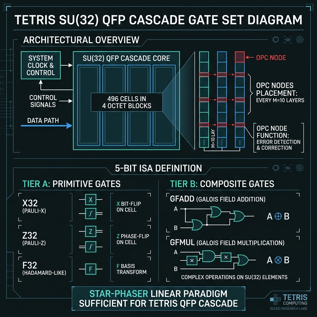
# tunable cells ≈ d(d−1)/2 = 496
Arbitrary U ∈ SU(32): O(d²) depth
Clifford generators: O(d) depth
Gate depth — not OPC bandwidth — is the primary quantum gate bottleneck. TETRIS is the first chip where 496 cells × 992 phase pairs forces hierarchical calibration (preview of NOVA ChiL).
GFADD | r3 = r1 ⊕ r2 (5-bit XOR) | depth 1 |
GFMUL | log + antilog mod 31 | depth 2 |
X₃₂ | |k⟩ → |k+1 mod 32⟩ | perm |
Z₃₂(θ) | |k⟩ → eiθ·k|k⟩ | phase ramp |
QFP-U(θ⃗) | one Reck cell | 496 LUT |
Log/antilog ROM: 31 × 5 bits × 2 tables — trivial in FPGA BRAM adjacent to die.
How we do it: Clements/Reck on 32 frequency modes; thermo-optic slow tuning + EO fast gates; 496 θᵢ in calibration LUT updated by GAP05 OPC-as-sensor; OPC every M=10 layers; offline SU(32) decomposition with Clifford+T library for QEC cycles.
SU(32) depth — primary quantum gate challenge · AWG resolution — readout/routing (flagged) · 992 phase pairs — calibration · ~32k FWM — secondary crosstalk · OPC bandwidth — not limiting at 1.55 THz
 T-05 · T-06
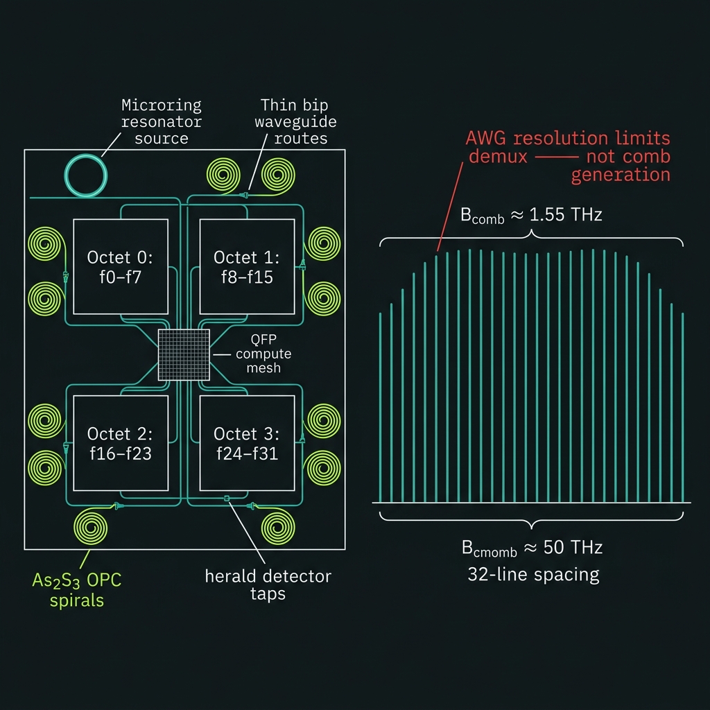
32-tooth phase-locked comb tile
S34 — heralded SFWM, octet tiling, localized As₂S₃ OPC.
Pump (1550 nm) → Si₃N₄ microring (Q>10⁵) → SFWM 32-line comb
    → EO flattening / missing-line fill → CEO lock → f_rep = 50 GHz
    → OPC boundary tap → 32-bin qudit channel

[Octet 0: f₀…f₇] [Octet 1: f₈…f₁₅] [Octet 2: f₁₆…f₂₃] [Octet 3: f₂₄…f₃₁]
↓ optional 4×8 ring pre-filter → unified 32-ch AWG demux- Si₃N₄ — routing, SFWM microring (0.01–0.1 dB/cm)
- As₂S₃ overlay — OPC spirals only (~55 mm Leff)
- TFLN / SiN EO — comb flattening, sideband injection
- No full-chip chalcogenide — loss tax minimized
- 32/32 lines within ±1 dB — hard gate
- Demux IL < 4 dB/ch — AWG-limited
- Crosstalk < −20 dB — S35
- OPC η per bin > 0.5 uniform ±10%
How we do it: AIM/KOTURA-class SiN MPW + post-process As₂S₃ at OPC sites; CEO from f-2f interferometer; K=8×T=4 herald mux inherited from GEMINI lineage; acceptance test samples 992 pairwise phases; pump reject before QFP entry.
 T-07 · T-08
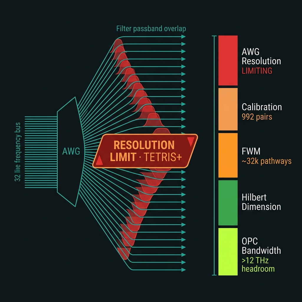
AWG resolution — the TETRIS ceiling
S35 — primary campaign flag for fab limits from TETRIS upward.
AWG resolution is the limiting fab factor from STAR-PHASER TETRIS upward. OPC bandwidth (>12 THz) and Hilbert dimension remain comfortable at d=32; spectral routing fidelity does not.
| AWG parameter | TETRIS target | GALAXY |
|---|---|---|
| Channel count | 32 | 16 |
| Spacing | 50 GHz | 50 GHz |
| 3-dB passband | ≥ 40 GHz | ≥ 45 GHz |
| Adjacent crosstalk | < −20 dB | < −18 dB |
| IL per channel | < 4 dB | < 3.5 dB |
At −20 dB crosstalk, leakage ≈ 1% per adjacent pair → ~31% cumulative leakage across 32 bins if uncorrected. OPC + calibration must witness and cancel leakage; otherwise SU(32) depth budget collapses.
Mitigation ladder: (1) single 32-ch AWG MPW · (2) 2×16 AWG tree (NOVA preview) · (3) 4×8 octet ring banks · (4) EO reconfigurable filters.
How we do it: AWG co-design with comb PLL (±1 GHz); measure 32×32 leakage matrix at fab test; feed GAP05 OPC-as-sensor correction; 32 SNSPD ports or 8× time-multiplexed readout; total readout IL < 6 dB target.
 T-09 · T-10
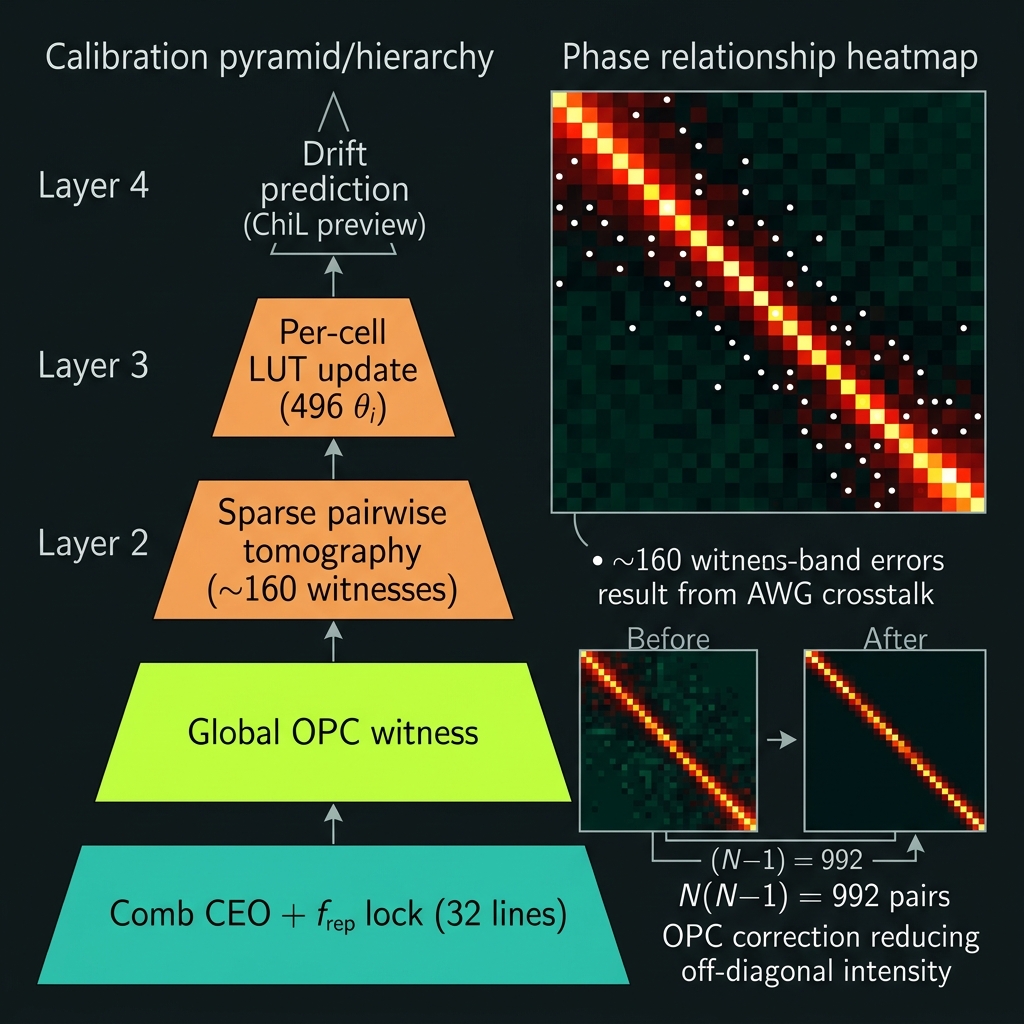
992 pairwise phase relationships
S36 — N(N−1) = 32×31; 4.1× GALAXY, 0.25× NOVA.
Each φij = arg(⟨fi|U|fj⟩) must be held to < 0.05–0.1 rad for >99% gate fidelity. Brute-force per-MZI sweeps over 496 cells take hours to days — TETRIS requires OPC-as-sensor self-calibration and sparse pairwise witness protocols.
Witness pairs: O(N log N) ≈ 160 measurements
→ infer full 992 via mesh Jacobian
496 θᵢ LUT · 1 kHz fast / 1 Hz full refresh
- Layer 0 — Comb CEO + f_rep lock (all 32 lines)
- Layer 1 — Global OPC witness (common-mode cancel)
- Layer 2 — Sparse pairwise tomography (~160 witnesses)
- Layer 3 — Per-cell LUT update (496 θᵢ)
- Layer 4 — Drift prediction (ChiL preview)
AWG coupling: resolution failure appears as off-diagonal φij for |i−j|=1 — calibration and routing limits are coupled. How we do it: boot CEO → rep → AWG align → OPC low-power; graph spanning witness set; static 32×32 leakage matrix stored at fab test.
 T-11 · T-12
More critical per bin — not more difficult
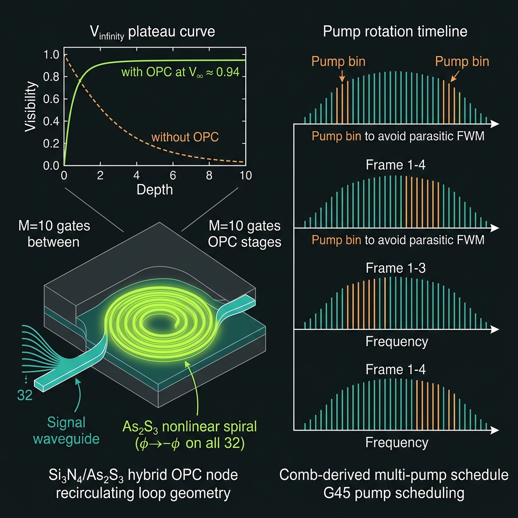
S37 — last pure STAR-PHASER OPC architecture before QUASAR.
| Platform | Si₃N₄ + localized As₂S₃ |
| η (single-pass) | 0.5–2% CW; 10–90% pulsed |
| Insertion | ~3 dB/pass → ~1 dB roadmap |
| Period | Every M=10 gates |
| Geometry | G1 recirculating loop |
OPC module physics unchanged; system role intensifies — 992 pairs amplify bin-nonuniform conjugation; ~32k FWM pathways increase parasitic pump coupling; AWG-limited routing means phase errors cannot be repaired by re-demuxing.
V_∞ ≤ exp(−M·σ²/(2η))   M=10, σ=0.08, η=0.5 → V_∞ ≈ 0.94
Target: η=0.9 pulsed, σ=0.05 → V_∞ ≈ 0.99
Comb-derived OPC (G45): each tooth k pumps neighbors (k±m); 32 simultaneous pump candidates — scheduled rotation across gate cycles minimizes ~32k pathway crosstalk. CV role: baseline squeezed vacua at encoding boundary; full distributed squeeze mesh deferred to NOVA+. How we do it: pump scheduling, Raman-null detuning, SBS guard, recirculating loop, OPC visibility feeds S36 witnesses.
 T-13 · T-14
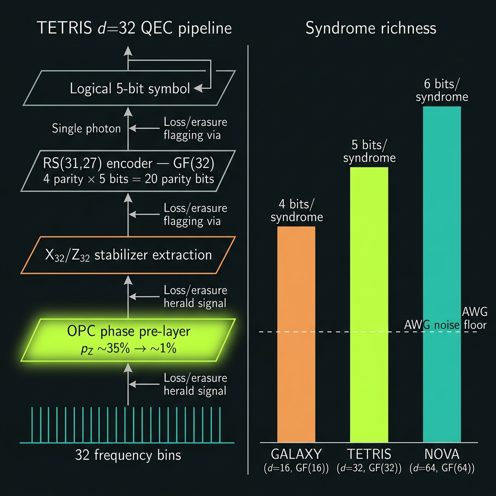
GF(32) syndrome richness
S38 — native finite-field QEC; OPC pre-layer, digital decode.
First STAR-PHASER chip with designed GF(32) Reed–Solomon, BCH, and qudit stabilizer layers. Each syndrome symbol carries 5 bits of diagnostic information vs 4 at GF(16) (GALAXY).
RS(31, 27): 4 parity symbols × 5 bits = 20 parity bits
Corrects t=2 symbol errors (d_min = 5)

X₃₂ |k⟩ = |k+1 mod 32⟩
Z₃₂ |k⟩ = ω^k |k⟩ ,  ω = e^{2πi/32}
Physical d=32 qudit → OPC phase pre-layer (every M=10, η≥0.5) → effective pZ ↓ (~35% → ~1% model) → GF(32) syndrome extraction → Berlekamp–Massey decode → logical correction. Loss from OPC IL + AWG IL → heralded erasure.
Syndrome mis-ID < 10⁻³/cycle requires XT < −20 dB AWG
How we do it: commit p(x)=x⁵+x²+1; ROM log/antilog + RS(31,27) generator polynomials; QFP projective measurement in Fourier basis; FPGA GF(32) decoder <1 µs; conjugate before syndrome round; SNSPD no-click → erasure flag.
 T-15 · T-16
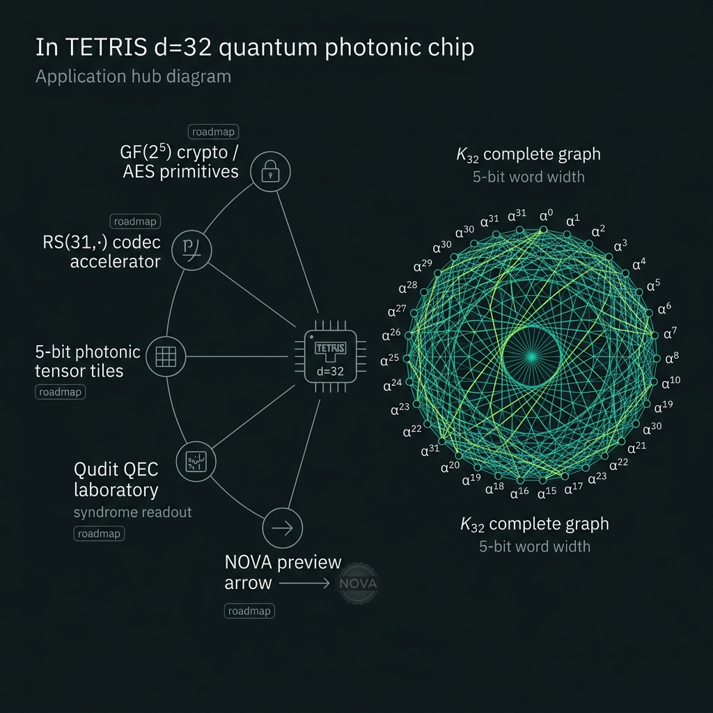
High-connectivity synthetic lattice
S39 — 32-vertex graphs, GF(32) crypto, 5-bit AI tiles.
- GF(2⁵) field arithmetic (AES-like primitives)
- RS(31,·) codec acceleration
- 5-bit photonic tensor tiles (G21 analog at m=5)
- K₃₂ — complete graph, full SU(32) mixing
- Q₅ — hypercube 2⁵, 5-bit flip gates
- C₃₂ — cycle, X₃₂ ring QEC
- Vertex k ↔ bin |fk⟩; edge (i,j) ↔ QFP coupling
TETRIS validates whether the 992-phase / AWG-limited / ~32k-FWM stack delivers utility before QUASAR NOVA fab cost. First chip where single-photon spectral dimension matches 5-bit computer word width without NOVA's 64-ch AWG tree.
How we do it: GF(32) SDK (GFADD/GFMUL + QFP-U API); lattice compiler |V|≤32 → coupling schedule; RS accelerator classical-only path; research mode exports syndrome + 992-phase telemetry; decimal I/O via G04 transcoder optional.
 T-17 · T-18
Bill of materials + control stack
Every component in the TETRIS d=32 system — photonics, electronics, lasers, materials — with vendor sourcing and foundry split.
Same split-fab as GEMINI & GALAXY
FEOL: LIGENTEC AN800 — Si₃N₄ waveguides, microring, 32-ch AWG, 496 QFP cells, f-2f interferometer. Encrypted GDS-II.
BEOL: QLT internal — As₂S₃ OPC overlay (~55 mm Leff), OPC nodes every M=10 gates, recirculating OPC loop.
Bond: QLT — TFLN/SiN EO for comb flattening and sideband injection, EO reconfigurable filters.
Backup foundry: AIM/KOTURA (cross-qualification per R18 memos).
32-ch AWG scaling stress test
AWG: 32-ch demux vs GALAXY's 16-ch — doubles spectral fan-out, stresses insertion-loss budget.
CEO lock: On-chip f-2f interferometer for carrier-envelope offset stabilisation — not present in GALAXY.
QFP mesh: ~496 Reck-decomposed QFP cells vs GALAXY's smaller mesh — 8× phase-count growth.
Same foundry: LIGENTEC AN800 primary, AIM/KOTURA backup. Identical FEOL/BEOL/Bond split.
LUV language → QIL middleware → FPGA firmware → photonic chip
The full control stack from user code to photon — scaled to 496 phase channels.
.luv source → run_freqbin_shot → QIL IR 0.1.0 bundle
dac.voltages[496+] → 496 Reck phases → crosstalk-corrected 0–5 V for AD5372 × multipleqfp_schedule[] → ordered unitary / phase_mask / permute stepsshot_contract → SNSPD herald pattern + post-selection probability
Santec TSL-570 CW pump (1550 nm) · Menlo C-fiber clock (100 MHz, 150 fs)
f-2f CEO lock · OPC spirals ~55 mm Leff · EO reconfigurable filters · recirculating OPC loop
Where TETRIS sits
Today's chip vs tomorrow's stress test
GEMINI is the shipping STAR-PHASER reference SKU. TETRIS is the roadmap scaling stress test — interest form for research partners and diligence.