How We Do It
manufacturing the STAR-PHASER and QUASAR photonic Chips
This page is dedicated as a complete walkthrough of QLT's room-temperature photonic quantum processor — every stage from the birth of a single photon to its measurement, the device physics behind each step, and the specific numbers that make it work. This page names the materials, mechanisms, and operating points we keep out of public materials.
Optical phase conjugation, inside the chip
Photonic qubits barely lose energy, but they accumulate coherent phase error as they propagate through real, imperfect circuits ● fabrication non-uniformity, thermo-optic drift, residual dispersion, crosstalk. On state-of-the-art silicon nitride this caps useful interferometric depth at roughly 50–100 gates before two-photon interference visibility collapses.
We insert optical phase conjugation (OPC) modules ● degenerate / near-degenerate four-wave-mixing (FWM) sections in a hybrid Si₃N₄/As₂S₃ waveguide ● periodically along the circuit. Each module produces the phase-conjugate of the traversing field, reversing accumulated phase distortion passively: no measurement, no ancilla qubits, no feed-forward, at room temperature.
The result: a circuit whose phase error is bounded by the spacing between modules, not by total depth. That single result is the entire platform ● and the same hardware, driven by bright light, becomes an OPC-stabilized AI accelerator.
Phase conjugation reverses distortion
E_out(ω) = E*_in(ω)
φ_idler  = 2·φ_pump − φ_signal
         = −φ_signal + const
A field that accumulated phase φ(ω) over a path is mapped φ → −φ. Re-propagating through the same (or a symmetric) medium adds +φ, netting zero. It is the integrated-optics analogue of telecom mid-span spectral inversion ● and, formally, a Loschmidt echo.
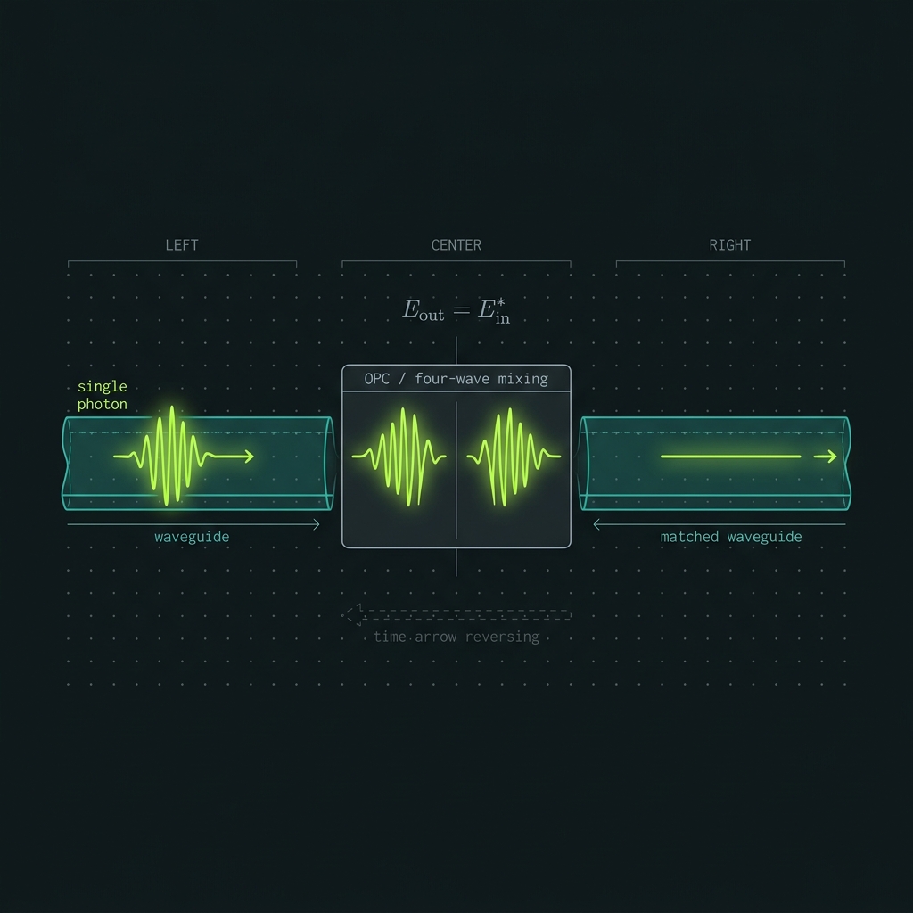 Figure 1
Ten stages, end to end
Follow one photon from creation to measurement. Each stage below is expanded in full technical detail.
Tap or hover any stage to expand its full technical detail. The journey runs in three phases — source & delivery, coherence & transport, then compute & readout.
Source & Delivery
Stages 0–3 · making a photon arrive on demandPump laser
→A telecom C-band laser at ~1550 nm is the only energy input to the entire processor. Nothing quantum is created from nothing — the pump supplies the photons that the χ⁽³⁾ nonlinearity later reshapes into correlated pairs. The line is intentionally linewidth-broadened to raise the stimulated-Brillouin-scattering threshold, then split and distributed to every source on the die.
~1550 nm · CW/pulsed · linewidth-broadened for SBS headroom · designed
Status: designed
Photon creation ● heralded SFWM
→Two pump photons annihilate inside a high-Q Si₃N₄ micro-ring and re-emit as an energy- and momentum-correlated signal+idler pair via the third-order Kerr nonlinearity (2ω_p = ω_s + ω_i). The ring (R ≈ 50 µm, Q > 5×10⁵) recirculates the pump thousands of times, and because four-wave mixing scales with the square of intensity, pairs are generated efficiently at milliwatt powers. Generation is fundamentally probabilistic.
Si₃N₄ micro-ring · Q>5×10⁵ · p ≈ 0.01–0.15 per pulse
Status: demonstrated (precedent)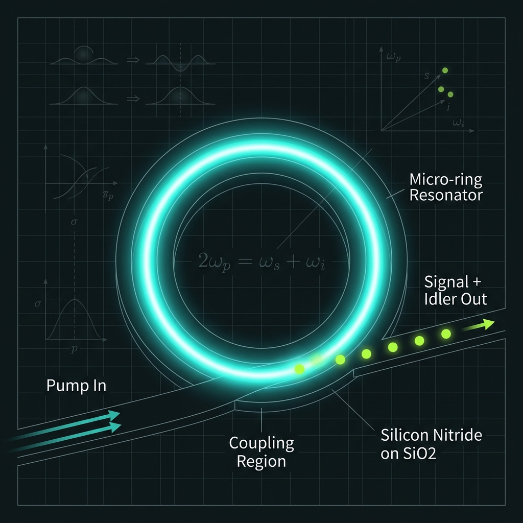
Heralding
→The idler photon is sent to a room-temperature single-photon avalanche diode (SPAD). Its click is a herald — proof that a usable signal photon exists in this exact time bin. The partner signal photon is parked in a low-loss delay spiral for a few nanoseconds while the electronics register the herald and decide what to do. Heralding turns a random event into a scheduled one.
Room-temp SPAD · ns-scale delay-spiral buffer
Status: designed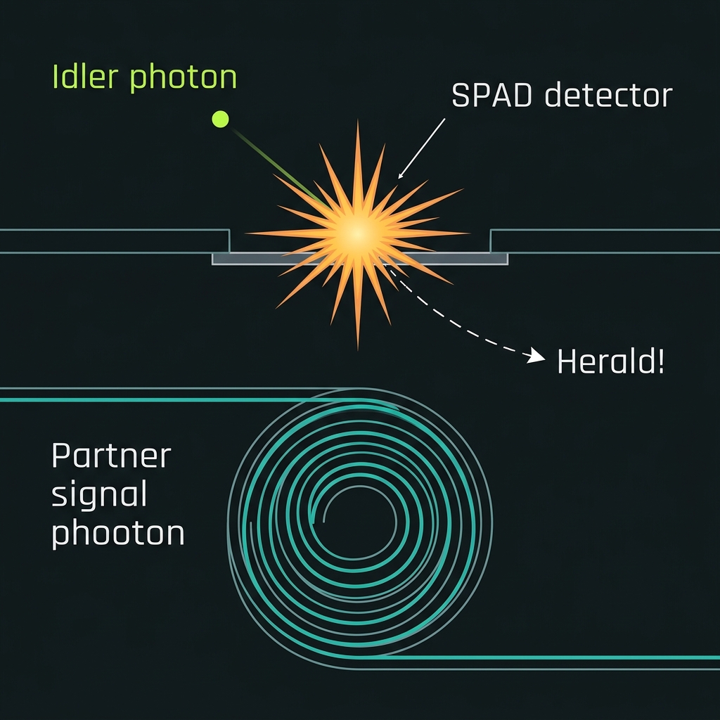
Active multiplexing
→One probabilistic source is unreliable; many in parallel are not. Eight heralded sources (K=8), each with four temporal retry slots (T=4), feed a binary switch tree. Herald clicks tell the controller which source and slot actually fired, and that one photon is routed to the shared output. Availability is designed to climb toward ~96.6% — a target from the model, not a measured result.
K=8 · T=4 · A = 1−(1−p)^(K·T) → ~96.6%
Status: designed (target)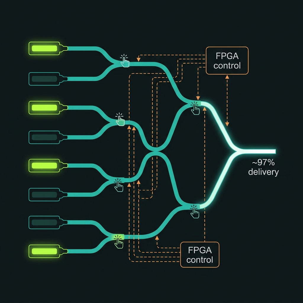
Coherence & Transport
Stages 4–6 · keeping the photon clean across the chipSource-stage OPC
→The first optical-phase-conjugation module reverses the photon's wavefront, erasing the route-dependent phase and dispersion it accumulated through a particular source and switch path. Afterwards, photons that came from different sources become mutually indistinguishable — the precondition for high-visibility interference in the gate mesh. OPC is an analog phase pre-layer, complementary to (not a replacement for) digital error correction.
FWM phase conjugation · route-phase + dispersion erased
Status: theory rigorous / to-be-tested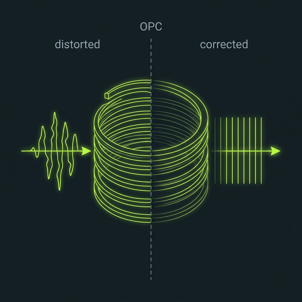
Low-loss backbone
→Ultra-low-loss stoichiometric Si₃N₄ waveguides carry the photon from the source region to the compute region. The 5.0 eV bandgap eliminates two-photon absorption at telecom wavelengths, and athermal routing holds the phase stable against temperature drift. Because photon loss is the dominant enemy of the whole architecture, the backbone is engineered toward sub-0.1 dB/cm propagation with minimal bends and crossings.
Stoichiometric Si₃N₄ · no TPA · athermal · <0.1 dB/cm target
Status: demonstrated (precedent) / target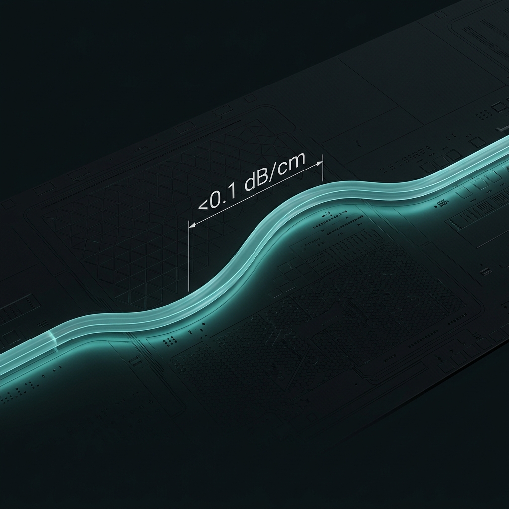
Encoding conversion
→An optional in-line transcoder converts the qubit among all six supported encodings — dual-rail, time-bin, frequency-bin, polarization, single-rail, and continuous-variable. It is invoked only at boundaries between subsystems that speak different encodings (memory, networking, hybrid CV/DV), so a single-encoding computation skips it entirely. Each conversion boundary is phase-corrected by an OPC element to pay back the phase error the transcoding introduces.
6 encodings · invoked only at cross-encoding boundaries · OPC-corrected
Status: optional capability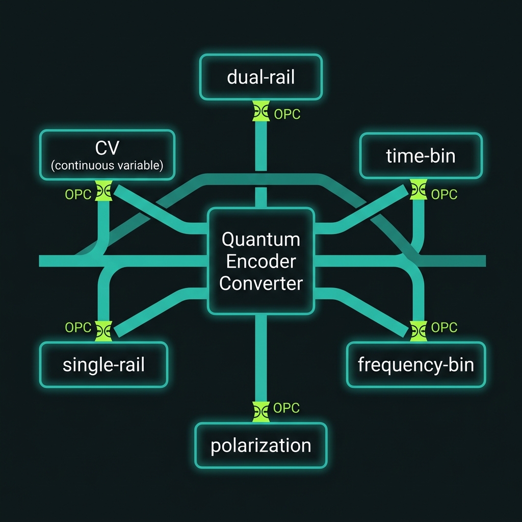
Compute & Readout
Stages 7–9 · gates, error bounding, and measurementMZI gate mesh
→A reconfigurable Clements mesh of Mach–Zehnder interferometers implements arbitrary linear-optical unitaries. Single-qubit gates are simply mesh phase programs; two-qubit entangling gates are realized through measurement-based fusion of resource states. The mesh is the programmable heart of the processor.
Clements MZI mesh · arbitrary unitary · measurement-based fusion
Status: demonstrated (precedent)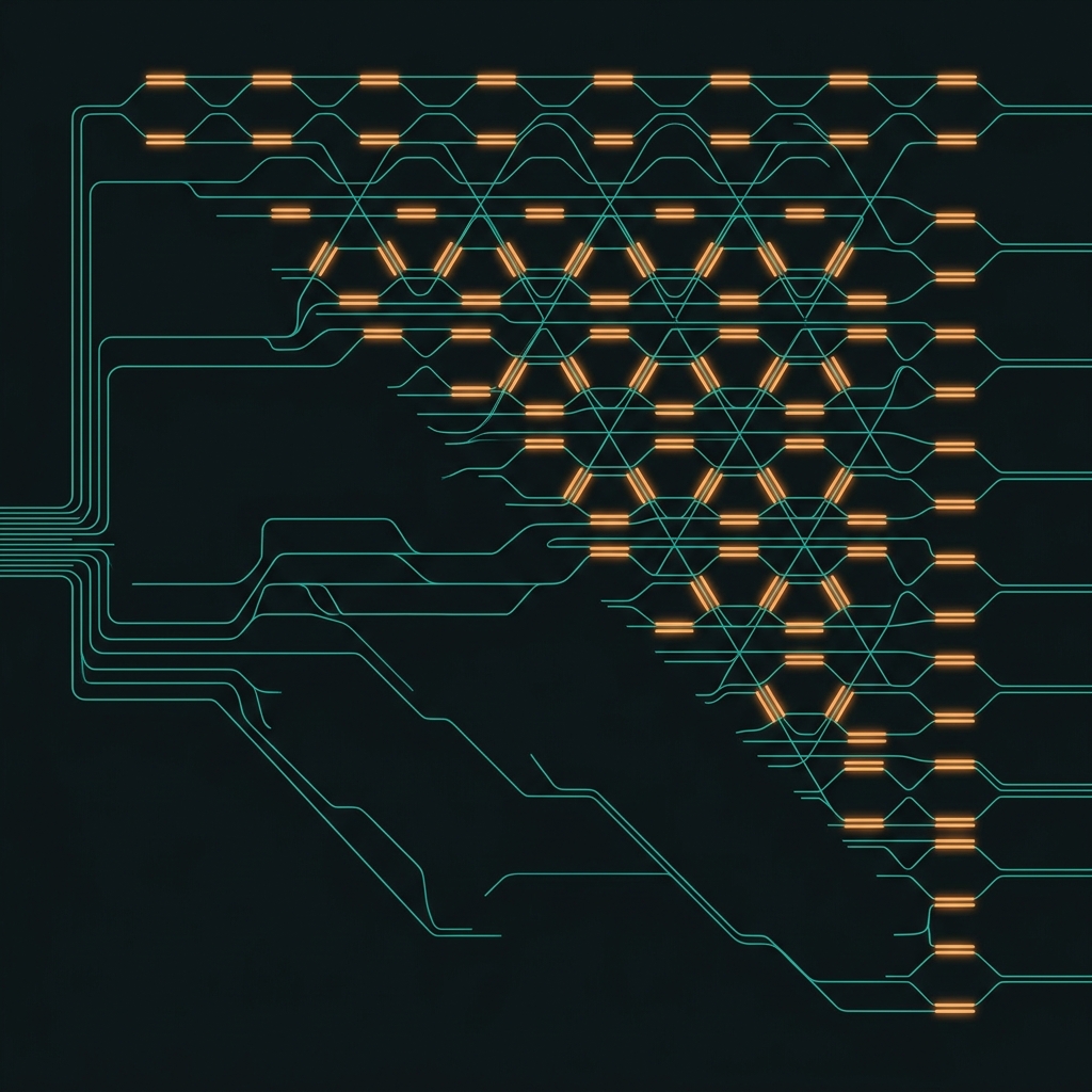
Periodic OPC lattice
→Roughly every ten gates, the photon re-enters an OPC spiral that conjugates and reverses the phase drift accumulated since the last correction. This bounds coherence error by interval rather than by total depth — the mechanism behind depth that is phase-depth-independent (V_∞ = exp(−Mσ²/2η)) and ultimately survival-limited, requiring η ≳ 50% and ~1 dB/pass jointly.
OPC every ~10 gates · error bounded by interval, not depth
Status: theory rigorous / to-be-tested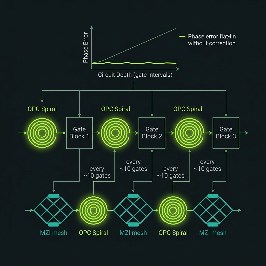
Feed-forward & detection
→Measurement clicks drive an FPGA that, within the feed-forward budget, fires the committed sub-nanosecond TFLN electro-optic switch (a ~150–175 fs piezo upgrade is verification-pending) to steer a partner photon still in flight — closing the measurement-based compute loop. Final readout is room-temperature: SPADs for discrete-variable encodings, or Ge-on-Si homodyne for continuous-variable.
FPGA feed-forward · sub-ns EO switch (committed) · SPAD / homodyne readout
Status: designed (EO) / verification-pending (piezo)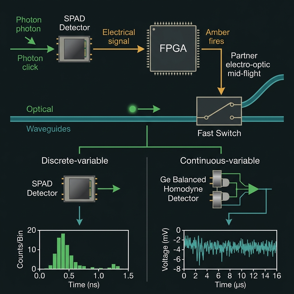
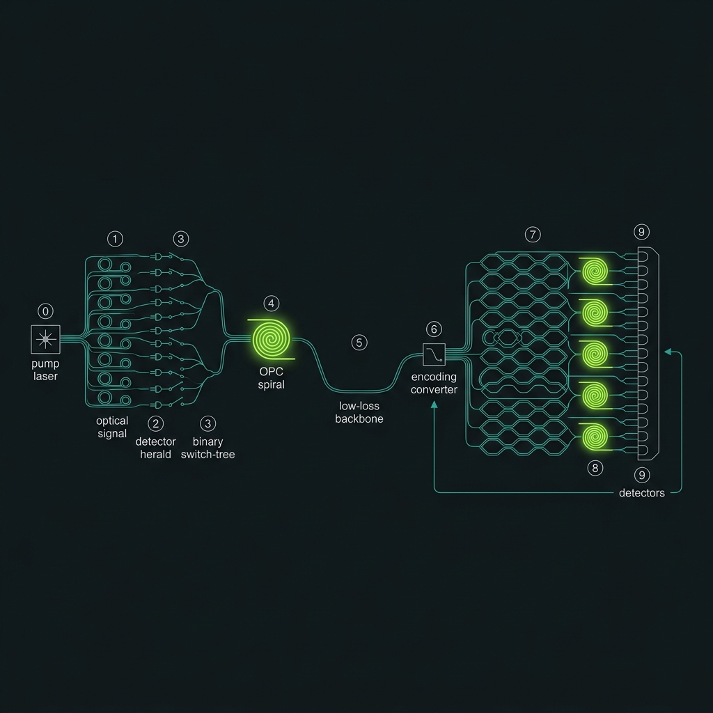 Figure 2
How a single photon is born
Heralded spontaneous four-wave mixing in resonant silicon nitride.
Spontaneous four-wave mixing (SFWM)
Inside a Si₃N₄ micro-ring resonator, two pump photons are annihilated and re-emitted as a correlated photon pair through the third-order (χ⁽³⁾) Kerr nonlinearity. Two conservation laws govern the process:
2·ω_pump = ω_signal + ω_idler      (energy)
Δk = 2k_p − k_s − k_i ≈ 0          (phase match)
|β₂| < 10 ps²/km at the pump        (dispersion)
The ring (R ≈ 50 µm, Q > 5×10⁵) traps the pump and lets it circulate thousands of times. Because FWM scales with the square of intensity, this resonant buildup makes pair generation efficient at milliwatt pump powers.
8 multiplexed rings · C-band · p ≈ 0.01–0.15/pulse
SPDC in Type-II ppKTP
For the MVP bench source we use a periodically-poled KTP crystal with a χ⁽²⁾ nonlinearity, where one higher-energy photon splits into two:
ω_pump → ω_signal + ω_idler
775 nm  → 1550 nm + 1550 nm
Poling period Λ ≈ 46.1 µm
This external source proves single-photon operation (g²(0) < 0.5), ~10⁶ pairs/s, >10% heralding efficiency ● validating the full chain before the harder on-chip SFWM integration. It is the lower-risk path for v1.
HOM > 85% · CAR > 50:1 · TEC-cooled, no cryogenics
Turning "maybe" into "now"
Pair generation is fundamentally probabilistic ● you cannot demand a photon on command. Because the two photons of a pair are correlated, detecting the idler on a separate path is an unambiguous flag that the signal photon exists. That herald click is what the rest of the architecture acts on: it triggers multiplexing routing and synchronizes the photon with classical control.
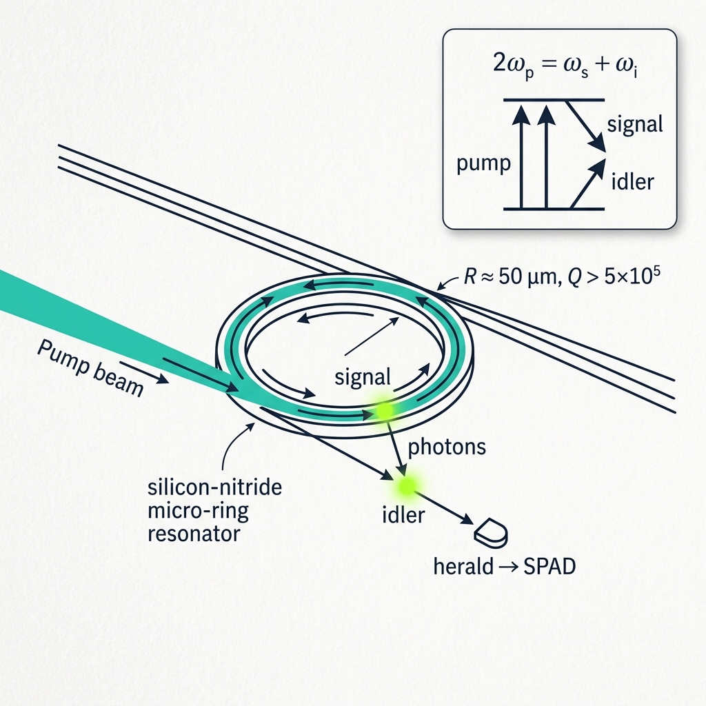 Figure 3
Beating the odds: active multiplexing
How probabilistic sources become near-deterministic delivery.
A single source firing 10% of the time is useless for computing ● ten simultaneous photons would arrive with probability 0.1¹⁰, one in ten billion. The fix is to run many sources in parallel and route whichever one fires:
P_success = 1 − (1 − p)^K          (spatial)
P_success = 1 − (1 − p)^(K·T)      (spatial × temporal)
Eight sources (K=8) feed a binary switch tree of log₂8 = 3 stages. Herald detectors tell the FPGA which source fired; the switches route that photon to a shared output. The photon waits in an on-chip delay spiral during the ~20–70 ns electronics decision. Every route is path-length-equalized to ±0.5 µm so photons remain indistinguishable.
spatial only
spatial × temporal (designed)
extinction >20 dB
rms, for HOM >99%
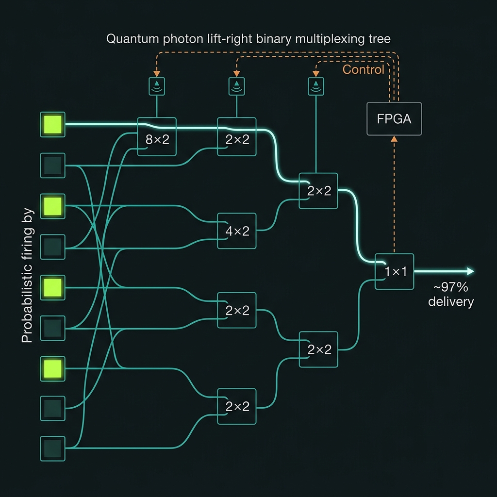 Figure 4
The hybrid Si₃N₄ / As₂S₃ waveguide
No single material satisfies all four quantum-grade OPC requirements at once. We co-optimize two.
| Property | Si₃N₄ (core / routing) | As₂S₃ (overlay / nonlinearity) | Role of the hybrid |
|---|---|---|---|
| Kerr n₂ | 2.4×10⁻¹⁹ m²/W | 2–5×10⁻¹⁸ m²/W (~10–20×) | As₂S₃ supplies nonlinear gain |
| Propagation loss | 0.01–0.1 dB/cm | 0.1–0.7 dB/cm (annealed) | Si₃N₄ supplies low-loss transport |
| Bandgap | ~5 eV (no TPA @1550) | ~2.4 eV (no TPA @1550) | Both two-photon-absorption free |
| CTE | 3.2 ppm/K | ~21.6 ppm/K | Mismatch → Patent 04 stress relief |
| CMOS compatibility | Native | Arsenic, back-end only | Split-fab isolation |
Localized overlay
Stoichiometric Si₃N₄ strip core (~800 × 400 nm) with As₂S₃ cladding (~500 nm) only at OPC nodes, reached by adiabatic tapers. ~50–60% of the mode sits in SiN, ~30–40% in As₂S₃.
Spiral ~5.5 cm in ~5 mm² · Euler bends · R_min ≈ 100 µm
Effective γ
γ_eff = (2π/λ)·(n₂,eff / A_eff)
Baseline (manufacturable): 3–5 W⁻¹m⁻¹. Optimized high-confinement: 8–15 W⁻¹m⁻¹.
CW η = (γ·P·L_eff)² ≈ 0.5–2% @ 100–200 mW
Generating the conjugate
A CW pump near 1550 nm drives the FWM that produces the phase-conjugate idler. Higher conversion (toward fault-tolerance-relevant regimes) uses pulsed pumping (1–10 W peak) or resonant enhancement.
Pump rejection ≥110 dB designed (provision ~120 dB w/ off-chip stage)
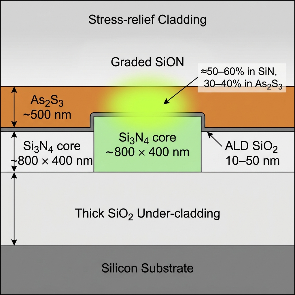 Figure 5
Why our chip design is hard to copy
A single photon is the faintest signal in nature. To protect it, we had to overcome three problems most teams never get past ● and the solutions are baked into our patented waveguide (Patent 10).
Unwanted "noise" light
The problem: Our laser is millions of times brighter than the single photons we compute with. A tiny fraction of that laser light can leak into the same channel and look like a real signal ● like static drowning out a whisper.
Our solution: We tune the chip to a precise "quiet zone" in the material where this leakage naturally cancels out. The result is a channel clean enough that fewer than 1 in 100 readings carries any stray noise.
The material fighting back
The problem: The high-performance material that powers our error correction has a quirk ● push too much laser power through it and it starts scattering light back at you, capping how hard we can drive the chip.
Our solution: Three engineering tricks ● spreading the laser's color slightly, subtly varying the channel's shape, and adding microscopic "sound barriers" ● together suppress the effect by more than 30×, so we can run the chip at full strength.
Wear over time
The problem: The same material is light-sensitive and can slowly degrade under intense light ● a reliability risk for any product that has to run for years.
Our solution: A protective manufacturing recipe ● a sealing layer, a stabilizing heat treatment, and a light-tight package ● that locks the material in and keeps performance stable for the long haul.
These three solutions are hard-won know-how that protect our moat. They are difficult to reverse-engineer, they are patented, and they are exactly what lets us run quantum-grade hardware at room temperature instead of inside a multi-million-dollar cryogenic freezer.
Exactly how each problem is solved
For the technical reader: the full mechanism, the design knobs, the numbers, and the trade-offs behind each fix.
Engineering a spectral "quiet zone"
What we're fighting. Pump light scatters inelastically off the glass's vibrational modes (phonons), producing a broad Raman background of Stokes (red-shifted) and anti-Stokes (blue-shifted) photons. Any one of these that lands in the signal or idler band is indistinguishable from a real qubit photon ● it raises g²(0), degrades heralding purity, and corrupts the coincidence-to-accidental ratio (CAR). Classical links shrug this off; a single-photon link cannot.
The four-part fix.
- Spectral placement at the Raman null. Chalcogenide's Raman gain is not flat ● it has minima between phonon bands. We set the pump–signal detuning to 7.0–7.8 THz (design point 7.4 THz), the low-Raman window of As₂S₃ measured by Collins et al. (Opt. Lett. 37, 3393, 2012; ~250× CAR improvement demonstrated there), so the FWM/OPC sidebands sit where spontaneous Raman is intrinsically weak.
- Exploiting the thermal (anti-Stokes) asymmetry. Anti-Stokes scales with phonon occupation n_th; Stokes with (n_th + 1). At 7.4 THz the phonon energy is ħΩ ≈ 30.6 meV versus k_BT ≈ 25.9 meV at 300 K, giving n_th ≈ 0.44. We place the heralded photon on the anti-Stokes side, which is suppressed by the n_th/(n_th+1) ratio even without cooling.
- Material partitioning. Si₃N₄ has far weaker Raman than As₂S₃. We generate and route photons primarily in the nitride and confine As₂S₃ to the short OPC/FWM gain sections only ● minimizing the photon's path length in the noisy material.
- Filter + time gate. A cascade of on-chip ring filters plus one spatially-separated off-chip stage is designed for ≥110 dB pump rejection (provision ~120 dB), and we only accept signal photons inside the narrow temporal window opened by the idler herald, rejecting out-of-gate Raman counts.
Trade-off: the Raman null is narrow, so the pump wavelength and waveguide dispersion must be co-locked to keep the FWM phase-match and the Raman null aligned. That co-design is part of the patented waveguide.
n_th(Ω) = 1 / (exp(ħΩ/k_BT) − 1)

ħΩ(7.4 THz) ≈ 30.6 meV
k_BT(300 K) ≈ 25.9 meV
⇒ n_th ≈ 0.44

P(Stokes)      ∝ (n_th + 1)
P(anti-Stokes) ∝  n_th
suppression    ≈ n_th/(n_th+1) ≈ 0.31
| Detuning window | 7.0–7.8 THz |
| Pump rejection | ≥110 dB designed (provision ~120 dB cascaded + off-chip) |
| Noise target | <0.01·η photons / mode (coupled to η) |
| Resulting CAR | >50:1 |
| Heralded g²(0) | <0.1 |
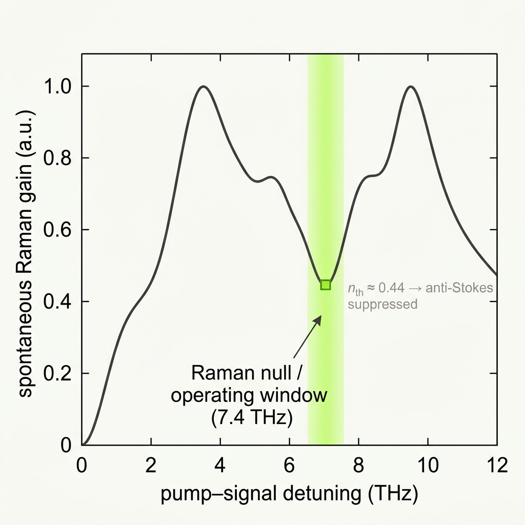 Figure 6
Raising the power ceiling 30×
What we're fighting. Via electrostriction, the pump drives an acoustic wave that reflects pump light backward as a Stokes wave; above a threshold this grows exponentially and clamps how much pump power we can put through the OPC section. Because OPC conversion efficiency scales with pump power (η ∝ (γPL)²), an SBS ceiling directly caps our error-correction strength. As₂S₃'s Brillouin gain g_B is ~100× that of silica, so the threshold arrives early:
P_th ≈ 21 · A_eff / (g_B · L_eff)
    ≈ 300–700 mW  (waveguide-corrected g_B,
                   narrow-linewidth CW)
    ≈ 120 mW      (bulk g_B, worst case)
The three-layer fix ● each attacks a different term:
- Pump linewidth broadening (attacks g_B). The Brillouin gain bandwidth is narrow (~tens of MHz). Broadening the pump from >200 MHz to ~1 GHz spreads its power across many Brillouin linewidths, cutting effective gain by roughly (1 + Δν_pump/Δν_B) ● about 10–30×. The catch is that OPC is phase-sensitive; we use a modulation format the conjugation process tolerates, because the idler inherits and partially self-cancels the pump's phase in the degenerate scheme.
- Longitudinal geometry dithering (attacks coherent buildup). We slowly vary the waveguide width along its length, which shifts the local Brillouin frequency Ω_B (it depends on effective index and acoustic velocity). With Ω_B sliding along z, no single frequency sees coherent gain over the full length ● the SBS interaction is de-phased and distributed, like apodizing a grating.
- Acoustic phononic-bandgap (APBG) trenches (attacks the phonon itself). Periodic air trenches / acoustic structures in the cladding open a phononic bandgap at Ω_B, so the required acoustic phonon literally cannot propagate. This removes SBS at its source and delivers >15 dB of suppression on its own.
Net result: stacking broadening + dithering + trenches lifts the effective SBS threshold by >30×, which is what unlocks pulsed pumping at 1–10 W peak and the high conversion efficiency η needed for deep, fault-tolerance-relevant OPC. Trade-off: trenches add thermal-management and mechanical-robustness constraints that feed back into the stress-relief design.
| Mechanism | Targets | Suppression |
|---|---|---|
| Linewidth broadening | gain g_B | 10–30× |
| Geometry dithering | coherent buildup | distributed |
| APBG trenches | acoustic phonon | >15 dB |
| Combined | ● | >30× threshold |
η_OPC ∝ (γ · P · L_eff)²
⇒ higher P-ceiling ⇒ higher η
Pulsed pump: 1–10 W peak
Pump linewidth: 200 MHz → ~1 GHz
A stability recipe for a reactive glass
What we're fighting. As₂S₃ has a bandgap near 2.4 eV (~520 nm). Photons at or above that energy ● and, at high intensity, two-photon and defect-assisted pathways even at 1550 nm ● reconfigure the amorphous network (homopolar "wrong" bonds), red-shifting the absorption edge and slowly raising C-band loss. For a product that must run for years, uncontrolled drift is a reliability killer.
The defense-in-depth recipe:
- Low-temperature PECVD SiO₂ cap. Deposited <150 °C (well under the ~210 °C glass transition) to seal the film from moisture and photo-oxidation without thermally damaging it.
- Densifying anneal, 130 °C / 24 h. A controlled pre-conditioning step that relaxes the metastable as-deposited structure and drives photodarkening toward its saturated state up front ● so the device ships already stabilized instead of drifting in the field.
- Optional ALD spacer. A thin atomic-layer-deposited interlayer at the Si₃N₄/As₂S₃ boundary (canonically SiO₂, 10–50 nm; Al₂O₃ as an adhesion variant) acts as a diffusion barrier and adhesion promoter, blocking interfacial reactions and stress-driven degradation.
- Pump power-density control. We keep optical intensity below the photodarkening onset by using a larger effective mode area in the As₂S₃ region and distributing nonlinear gain over length rather than concentrating it.
- Opaque hermetic packaging. A light-tight, moisture-sealed package blocks ambient visible/UV ● the most damaging wavelengths, being nearest the bandgap.
Roadmap lever: composition tuning (sulfur-rich As₂S₃ or Ge-As-S glasses) offers further intrinsic photostability if a given product line demands an even longer service life. Trade-off: every step here is temperature-capped by the As₂S₃ already on the wafer ● which is exactly why our process flow deposits it last (the fabrication "golden rule").
| Step | Spec | Purpose |
|---|---|---|
| SiO₂ cap | PECVD <150 °C | seal / oxidation barrier |
| Anneal | 130 °C / 24 h | pre-saturate darkening |
| ALD spacer | SiO₂ 10–50 nm (Al₂O₃ opt.) | adhesion / diffusion barrier |
| Power density | below onset | avoid driving darkening |
| Package | opaque, hermetic | block visible/UV + moisture |
Bandgap E_g ≈ 2.4 eV (~520 nm)
T_g(As₂S₃)  ≈ 210 °C  → all post-
            processing stays <150 °C
Why depth stops mattering
The error-bounding theorem that defines the platform (Patent 08).
Error grows with depth
Var(φ) = N · σ²
V(N)   = exp(−N·σ²/2)
With σ ≈ 0.05–0.15 rad per component, visibility drops below 90% by ~50–100 components. Usable circuit collapses.
Error reaches a bounded steady state
|ψ_out⟩ = √η|conjugate⟩ + √(1−η)|unconjugated⟩
Var_eff(segment) = (1−η)·M·σ²
recurrence: V_k ≤ (1−η)·V_{k−1} + σ²_seg
⇒  V_∞ ≤ σ²_seg / η = M·σ² / η
Bounded by interval M and conversion η ● not by total depth N. That is the entire thesis in four lines.
What OPC does and does not do
Corrects: coherent phase / dephasing ● the dominant error in interferometric photonic circuits.
Does not correct: photon loss (each pass adds ~3 dB) or depolarizing/bit-flip errors. OPC is a pre-layer that lowers the raw phase-error rate; full fault tolerance still pairs it with digital QEC (surface / LDPC / GKP).
Best geometry: cancellation is most rigorous in recirculating / symmetric layouts where the conjugate re-traverses the same static errors.
Open milestone: single-photon OPC coherence preservation in an integrated waveguide is theoretically supported (Gaeta & Boyd, 1995) but not yet experimentally demonstrated ● it is our #1 validation target, and the ">92% visibility at 1,000 gates" figure assumes η well above the 1–2% CW baseline.
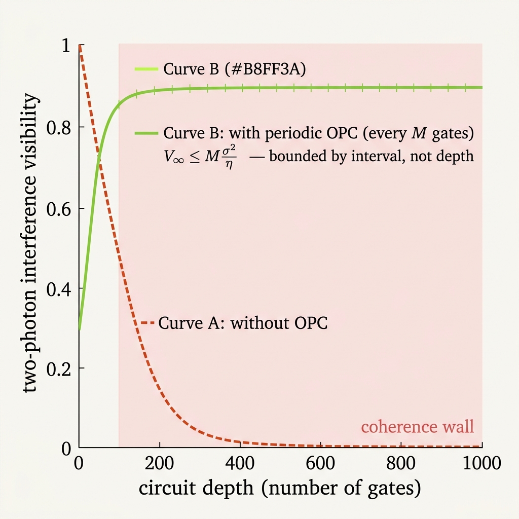 Figure 7
Full signal flow & the two-layer error stack
OPC is not the end of error correction — it is the first layer. Here is the complete photon pipeline and the precise division of labor between analog phase pre-correction and digital quantum error correction above it.
The complete signal pipeline — heralded source → OPC → fusion gates → digital QEC
| # | Stage | What happens | Error introduced | OPC's role |
|---|---|---|---|---|
| S0 | Pump laser | CW/pulsed ~1550 nm distributed on-chip; linewidth broadened ≥200 MHz–1 GHz for SBS headroom | — | — |
| S1 | SFWM source | Si₃N₄ microring (R ≈ 50 µm, Q > 5×10⁵) generates correlated signal + idler via χ⁽³⁾; p ≈ 0.01–0.15/pulse | g²(0) purity, spontaneous emission, spectral indistinguishability | — |
| S2 | Herald | Idler → room-temp SPAD click → gates signal into delay spiral; registers pair generation | Dark counts (<20 kHz DCR), timing jitter (<100 ps) | — |
| S3 | Active multiplexer | K=8 sources × T=4 temporal retries in 3-stage binary switch tree; herald click selects the one photon that fired → ~96.6% delivery | Route-dependent phase; per-stage IL <0.5 dB; path-length residual ≤0.5 µm | — |
| S4 | Source-stage OPC | First FWM conjugation module erases route-dependent phase and residual dispersion from the switch tree; photons from all 8 sources become mutually phase-indistinguishable — the precondition for high-visibility multi-source fusion | OPC insertion loss ~3 dB/pass; spontaneous FWM noise n_noise <0.01/mode | Pre-correction #1: erase mux-path signature before entering gate mesh |
| S5 | Low-loss backbone | Stoichiometric Si₃N₄ routing; no TPA at 1550 nm; athermal <0.1 dB/cm target; phase stable across temperature excursions | Propagation loss, thermo-optic drift (dn/dT ≈ 1.8×10⁻⁵ K⁻¹), residual GVD | — |
| S6 | Encoding conversion (optional) | Transcoder among dual-rail / time-bin / frequency-bin / CV; invoked only at cross-encoding boundaries (memory, networking) | Encoding-boundary phase, group-delay mismatch | OPC at each boundary reverses encoding-induced phase (GAP04 claims 12–13) |
| S7 | MZI fusion gate mesh | Clements mesh: 28 MZIs, 32 thermo-optic heaters → arbitrary 8×8 unitary. Single-qubit gates = mesh programs. Two-qubit gates = Type-I / Type-II fusion (probabilistic Bell-state measurement on resource states via HOM interference on a beamsplitter), with feed-forward to condition subsequent gates on the measurement outcome | σ ≈ 0.05–0.15 rad/component (fab non-uniformity + thermo-optic drift); HOM visibility falls as V(N) = exp(−Nσ²/2) — collapses below 50% past ~200–400 components without correction | — |
| S8 | Periodic OPC lattice | OPC module every M ≈ 10 gates conjugates accumulated phase; bounds V∞ ≤ Mσ²/η — depth-independent. Geometry: recirculating loop so conjugate re-traverses the same static errors exactly (Theorem 1, A303) | ~3 dB insertion loss/pass (arrives as heralded erasure); spontaneous FWM noise within noise budget | Pre-correction #2: in-circuit periodic phase rebounding; converts depth-limited to depth-scalable |
| S9 | Measurement + feed-forward | SPAD click → 64 ps TDC timestamp → FPGA BRAM lookup (1 cycle @ 200 MHz) → DAC + TFLN EO switch fires within ~11.2 ns total loop; steers partner photon still in delay spiral; closes the MBQC compute loop | SPAD jitter <100 ps; FPGA decision latency ~5 ns; residual timing jitter <0.8 ps RMS | — |
| QEC | Digital QEC layer | Surface / LDPC / GKP codes encode logical qubits in many physical qubits; syndrome measurements detect residual errors; classical decoder (FPGA + host) computes and applies corrections. OPC's own loss arrives as heralded erasure (known location → threshold ~25–50% vs ~1% for unheralded Pauli) | Overhead: 10–1,000× qubit count (surface code); decoder latency ~µs (off critical path); qubit throughput scales with code distance | OPC pre-correction lowers the physical error rate fed into QEC — the categorical difference between infeasible and feasible fault tolerance |
Layer 1: OPC (analog, passive). Layer 2: digital QEC. Together: fault tolerance.
Two mechanisms attack two different error channels. Neither is sufficient alone — and the specific value of their combination is that OPC moves the physical error rate from above to below the QEC threshold.
Corrects: coherent phase / dephasing (Z-type errors)
OPC targets the dominant error in interferometric photonic circuits: deterministic, coherent phase accumulation — fabrication offsets and thermo-optic drift that build linearly with depth. Because it conjugates without measuring the qubit, it introduces no back-action and does not collapse superpositions.
V∞ ≤ M·σ² / η          (bounded, depth-independent)
η_eff = 1−(1−η)^K_loop (recirculating enhancement)
Recommended point: η_eff ≈ 0.40, M = 10, σ = 0.08 rad
→ V∞ ≈ exp(−10·0.064/0.40) ≈ 0.85    [model / to-be-tested]
Does NOT correct: photon loss (~3 dB/OPC pass — this shows up as heralded erasure, not lost information), fast uncorrelated phase noise, bit-flips (X errors), or depolarizing noise. Those go to Layer 2.
Corrects: residual phase, loss, bit-flip, depolarizing
Three code families, each matched to a different regime:
- Surface codes (XZZX biased variant). Threshold ~0.7–1% Pauli error rate. OPC reduces the raw Z-error probability from ~35.7% at 1,000 gates (uncorrected) to ~1.2% (with OPC @ η_eff = 0.40, M = 10) — a categorical infeasible→feasible shift. Biased surface codes add 1.8–5.7× further overhead reduction by exploiting the Z-dominant error model OPC leaves behind.
- qLDPC codes. Lower qubit overhead than surface codes by ~20–80× at the same logical error rate. Target for deeper circuits where surface-code resource costs are prohibitive.
- GKP codes (Gottesman–Kitaev–Preskill). Native to continuous-variable / squeezed-light modes; encode a qubit in the phase space of a harmonic oscillator. OPC-preserved squeezing contributes +2.5–10 dB of effective noise reduction on top of GKP syndrome extraction — the two corrections are synergistic.
OPC's own insertion loss arrives as heralded erasure (loss detected = location known → threshold ~25–50%) rather than unheralded Pauli error (~1% threshold) — making OPC's dominant side-effect ~25–50× cheaper for QEC to correct than if it were random dephasing.
WITHOUT OPC (N = 1,000 gates, σ = 0.08 rad):
  p_Z ≈ 1 − exp(−N·σ²/2) ≈ 1 − exp(−3.2) ≈ 95.9%
  → far above surface code threshold
  → circuit at 1,000 gates: INFEASIBLE

WITH periodic OPC (η_eff = 0.40, M = 10, σ = 0.08):
  V∞ = exp(−M·σ²/η) = exp(−0.016/0.40) ≈ 96.1%
  p_Z,eff ≈ 1 − V∞ ≈ 3.9%            [model]
  → just above threshold; biased codes bring to ~1–2%
  → 1,000-gate circuit: FEASIBLE with QEC

OPC contribution: 96% raw error → <2% corrected error
— a categorical shift, not a marginal improvement.
Status: [model]. Numbers from WS5/A510 Stim+PyMatching schematic analysis. The gating experiment that makes these into [demonstrated] numbers is the integrated single-photon HOM-before/after OPC demonstration on a dual-rail Sagnac node (campaign #1 milestone, T9 in the GAP03 quantum test protocol).
| Error type | Corrected by | How |
|---|---|---|
| Coherent phase / Z-drift | OPC (Layer 1) | FWM phase conjugation; passive, no measurement |
| Photon loss | QEC (Layer 2) as erasure | Heralded = known location → 25–50% threshold |
| Bit-flip (X error) | QEC (Layer 2) | Stabilizer syndrome + correction |
| Depolarizing (mixed Pauli) | QEC (Layer 2) | Surface / LDPC code |
| CV squeezing degradation | OPC + GKP (both layers) | OPC preserves squeezing → GKP syndrome uses the extra squeezing margin |
Why HOM visibility — and therefore OPC — is the central figure of merit
QLT uses the linear optical / fusion-based quantum computing (LOQC / FBQC) model. Two-qubit logic is not a deterministic nonlinear gate — it is a probabilistic Bell-state measurement (fusion) on resource states, with the FPGA performing feed-forward corrections so the overall logical operation is deterministic even though each fusion attempt succeeds only half the time.
Type-I fusion: one-photon measurement on two resource qubits; implements a controlled-X / CZ-like operation in the cluster-state frame; succeeds with probability ½.
Type-II fusion: two-photon Bell-state measurement (PBS + two SPADs); directly projects two dual-rail qubits into a Bell state; succeeds with probability ½ for ideal linear optics, improved by photon-number-resolving ancilla or adaptive boosting.
In fusion-based quantum computing (FBQC), the entire computation is decomposed into a network of fusions on a sequence of small resource states (e.g. 6-ring graphs). Because fusions fail half the time, fault-tolerance is achieved not by avoiding failure but by generating resource states at sufficient rate that enough fusions succeed to maintain the logical computation. The overhead in resource-state generation is where photon source availability (Stages S1–S3) and OPC-preserved indistinguishability (Stage S4) become critical.
Fusion is HOM interference: two photons on a 50/50 beamsplitter. Distinguishable photons (mismatched phase, spectrum, or timing) produce classical two-photon output; indistinguishable photons bunch. The fusion success probability (and thus the logical gate fidelity) scales as:
F_fusion ≈ ½(1 + V_HOM)
V_HOM    ≈ V_spectral · exp(−N·σ²/2)

Without S4 OPC: V_HOM collapses past ~50–100 gates
With S4 OPC:    route-phase erased → V_HOM ≈ V_spectral
                (spectral purity the only remaining limit)
Source-stage OPC is what allows photons from 8 different multiplexed paths to arrive at the fusion beamsplitter with matched phase — so the fusion fidelity is bounded by spectral indistinguishability, not by how many switches the photons traversed.
Benchmark: PsiQuantum 99.22% same-chip fusion fidelity (Nature 2025) — achieved with well-controlled photon indistinguishability, the level this architecture targets
Gates, feed-forward, and detection
Reconfigurable MZI mesh
A Clements/Reck mesh implements any N×N unitary from N(N−1)/2 beam splitters + phase shifters. v1 flagship: 8-mode, 28 MZIs, 32 thermo-optic heaters. Single-qubit gates are mesh programs; two-qubit gates are measurement-based fusion (not deterministic χ⁽³⁾ CZ).
Ultrafast switching (technology-agnostic)
A measurement click → FPGA logic → qualified ultrafast switch (committed v1: TFLN electro-optic; verification-pending piezo upgrade species) fires within the feed-forward budget (>20 dB extinction, <0.5 dB loss designed) to reroute or phase-shift a partner photon while it waits in a delay line. This closes the measurement-based computing loop.
Room temperature, no cryogenics
InGaAs/GeSi SPADs for discrete-variable counting (≥28% PDE, <20 kHz dark count, <100 ps jitter). Ge p-i-n balanced homodyne (15.3 GHz) for continuous-variable readout, with the local oscillator drawn from the same pump ● no external phase-lock loop.
Turning a photon into an electron you can read
"Using" a photon means converting it to electricity. Two paths, opposite amplification philosophies.
A 1550 nm photon carries ~0.8 eV. Absorbed in a sub-bandgap semiconductor (InGaAs E_g ≈ 0.75 eV, or Ge/GeSi), it promotes one electron to the conduction band, creating a single electron–hole pair. That is the conversion — but one pair is far too faint to read, so each path below amplifies it differently.
Photon counting with SPADs
For qubit logic we ask "did a photon arrive, and when?" An InGaAs/GeSi single-photon avalanche diode is reverse-biased 3–5 V above breakdown — a hair-trigger "Geiger mode." The lone photo-electron is accelerated until it impact-ionizes the lattice, triggering a self-multiplying avalanche (gain ~10⁶) that turns one photon into a milliamp-scale click.
SiN bus → Y 50:50 tap → Euler S-bend
       → mode expander (900→1500 nm) → SPAD
+25 V ─ 500 Ω quench R ─ anode ─→ TDC (LVDS)
detect 1.2 ns · quench 5 ns · hold-off ~35 ns
Light leaves the waveguide through a low-loss tap (<0.45 dB); an active-quench circuit re-arms the diode; a TDC ASIC time-stamps every click at 64 ps and streams it to the FPGA. The timestamp is the data — it yields g²(0), HOM visibility, coincidences, and heralding.
Quadrature readout with balanced homodyne
For squeezed-state qumodes the information lives in the field's quadrature, not in a click — so avalanche gain is the wrong tool. Instead the faint signal is mixed on a 50:50 coupler with a bright local oscillator split from the same pump (inherently phase-locked, no external PLL).
signal ─┐
        ├─ 50:50 ─→ Ge p-i-n  ┐
LO ─────┘        ─→ Ge p-i-n  ┴─ subtract → TIA
i₁ − i₂  ∝  selected quadrature × LO gain
readout bandwidth: 15.3 GHz
A matched pair of linear Ge p-i-n photodiodes detects the two outputs; the difference current cancels the LO's classical noise and leaves a signal proportional to the chosen quadrature, amplified by the strong LO. A transimpedance amp delivers it to high-speed pads at 15.3 GHz.
Detection isn't only final readout — it's how the chip computes. In measurement-based logic a click becomes electrons, the FPGA reads them, and within the feed-forward budget it fires a femtosecond switch to steer a partner photon still in flight. Photons → electrons → decision → photon steering is the actual gate cycle. And because both detectors (avalanche SPAD, p-i-n homodyne) run at room temperature, this entire optical-to-electrical stage stays in the warm core — no cryogenic SNSPDs at 1–4 K. A portfolio option (P1 §4.2) also allows up-converting telecom photons to a visible band for higher-performance silicon detectors.
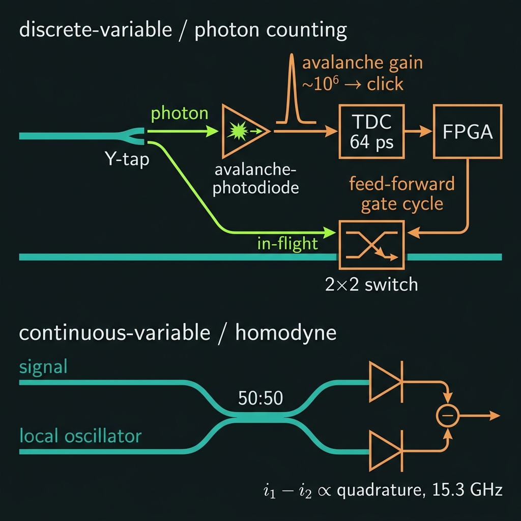 Figure 8
Encoding dimensionality: qubit vs. qudit
How many bits one photon can carry ● the "base" of our encoding ● and how far each scheme scales.
Our native unit is the qubit ● base-2, two levels, one bit per photon. "More bits" means a higher-dimensional qudit: a d-level photon carries log₂d bits, so the levels you need grow exponentially with bits.
Today's flagship is an all-qubit (base-2) machine. Higher dimensions are a roadmap extension, not v1 ● but the key point is that our OPC error-correction layer is broadband enough that it is not the thing that limits going high-dimensional.
Why frequency-bin is the strongest high-d path: per Patent 08 [0090], frequency-bin structure survives OPC "as long as the FWM bandwidth exceeds the bin spacing" ● and our measured FWM bandwidth is >12 THz (>100 nm in As₂S₃). With GHz-class bin spacing, one OPC module can phase-conjugate thousands of bins at once. The usual high-dimensional bottleneck ● phase-error accumulation ● is the part we already solved.
d = 2^bits      bits = log₂ d
1 bit  → d = 2     (qubit ← today)
2 bits → d = 4     (ququart)
3 bits → d = 8
4 bits → d = 16
10 bits → d = 1024 (bleeding edge)
| Encoding | Native | High-d path | Practical ceiling | What limits it |
|---|---|---|---|---|
| Polarization | d = 2 | none | 1 bit (hard limit) | only two orthogonal states exist |
| Dual-rail (path) | d = 2 | multi-rail (d waveguides) | ~2–4 bits (d=4–16) | mesh area ~d², d modes per symbol |
| Time-bin | d = 2 | multi-time-bin | ~a few bits | delay-line loss, detector jitter |
| Frequency-bin | d = 2 | frequency-comb qudits | ~3–6+ bits (d≈10–100+) | bin-resolved gates & detection |
| Continuous-variable | analog | quadrature capacity | ~a few bits/mode | squeezing (4–7 dB on-chip) |
1 bit (base-2) is today. 2–4 bits (d=4–16) is a credible near-term roadmap via frequency-bin (secondarily time-bin / multi-rail). ~6 bits is plausible in combs. 10 bits (d=1024) is bleeding-edge ● gated by qudit state preparation, gate sets, crosstalk, and high-dimensional detection, not by our OPC layer. CV gives analog multi-bit density but is squeezing-limited (fault-tolerant CV wants 11.5–13 dB vs. ~7–10 dB inferred on-chip today).
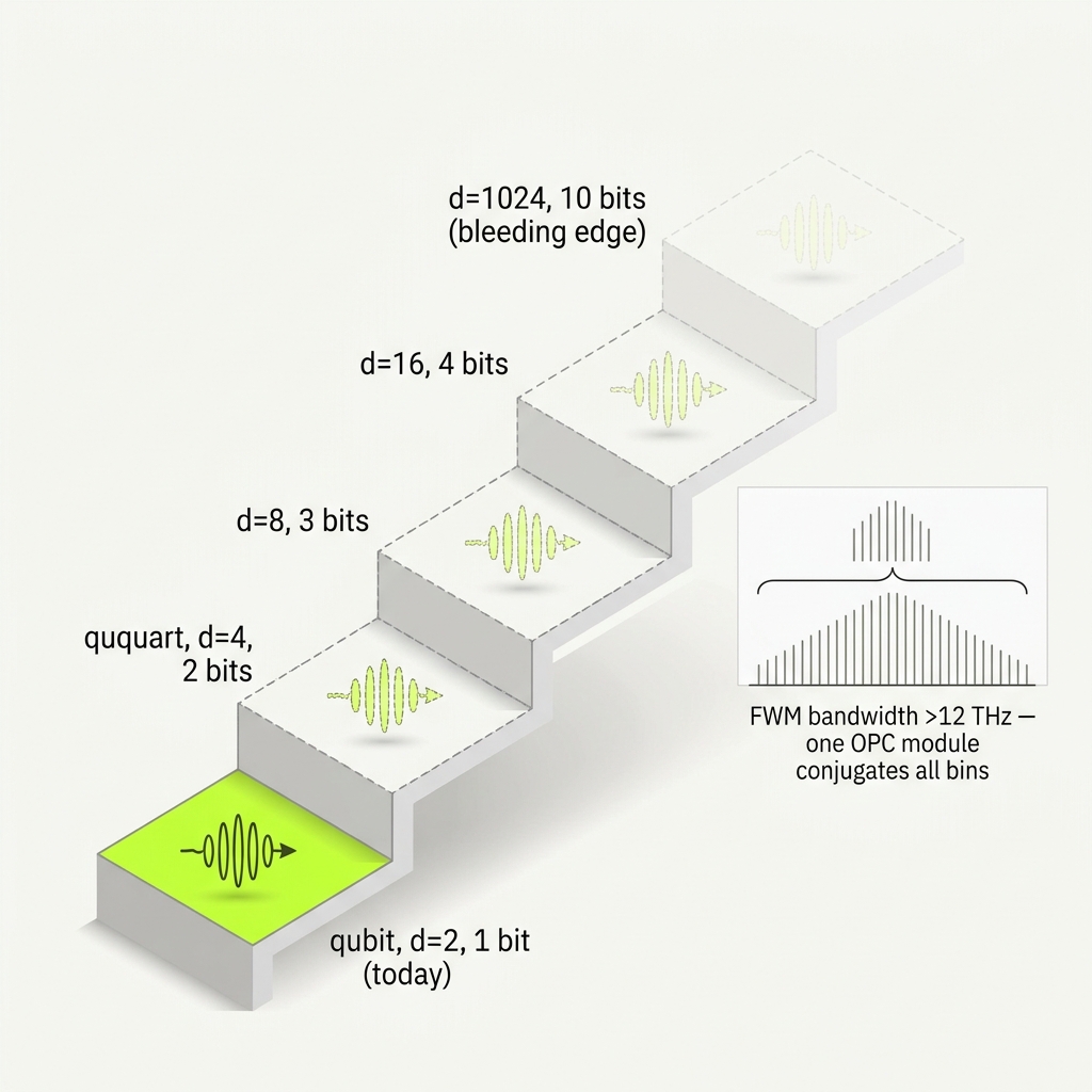 Figure 9
The upgrade path: from two rails to ten colors
How a base-2 dual-rail qubit is promoted into a base-10 frequency-bin "decit" — without leaving the chip.
Today the processor runs in dual-rail: a single photon sits in one of two waveguides — path A is |0⟩, path B is |1⟩ — so one photon carries exactly one bit (base-2). To reach base-10 we do not change the photon and we do not add nine more wires. We change what we read off the photon: instead of counting paths, we count colors. A photon prepared across ten evenly-spaced frequency bins from the on-chip comb can occupy any one of ten levels, |0⟩…|9⟩ — a single decimal digit living in one photon, in one spatial channel. The same OPC layer that already protects the dual-rail mesh is broadband enough to protect all ten colors in a single pass — which is the whole reason the jump is even on the table for us.
One photon, two waveguides. |0⟩ = path A, |1⟩ = path B. Single-qubit gates are programs on the 8-mode Clements mesh (28 MZIs, 32 thermo-optic heaters); two-qubit gates are measurement-based fusion. 1 bit / photon. (v1 demonstration target.)
An on-chip converter (cascaded micro-ring add-drop filters, an AWG, or an electro-optic modulator — Patent 11) maps the two paths onto two colors: |0⟩ = f₁, |1⟩ = f₂. An OPC pass sits at the conversion boundary and resets the phase error it introduces — "regardless of the number of conversions" (Patent 11 [0064]/[0084]). Same qubit, now riding frequency. (Design / patent claim.)
Drive ten bins from the spectral lattice instead of two. The photon now occupies any of |0⟩…|9⟩ — one decimal digit, ≈ 3.322 bits in a single photon (log₂10), in one spatial mode. This is the radix-10 unit of Spectral Decimal Computing. (Roadmap extension, not v1.)
Nothing stops at ten. d = 16, d = 100+, ultimately thousands of bins across the >12 THz window — each photon a denser register, still in one waveguide. The ceiling is set by gates and detection, not by the carrier. (Forward-looking.)
BASE 2  ·  dual-rail (paths)          BASE 10  ·  frequency-bin (colors)
  path A ──────────▶ |0⟩                f₀ f₁ f₂ f₃ f₄ f₅ f₆ f₇ f₈ f₉
  path B ──────────▶ |1⟩                 0  1  2  3  4  5  6  7  8  9
  1 photon = 1 bit                       1 photon = 1 decimal digit  (≈3.322 bits)
  state space: 2^N                       state space: 10^N   (N digits)
Binary processors decompose every decimal quantity into base-2 and pay for it in gate count. A frequency-bin photon is natively ten-dimensional, so a decimal digit can be encoded directly into ten optical frequency modes — no binary decomposition. The state is |ψ⟩ = Σₙ cₙ|fₙ⟩ and it evolves under SU(10) rather than SU(2):
- The "X" gate becomes a digit shift. X₁₀|n⟩ = |n+1 mod 10⟩ — implemented by an electro-optic frequency shifter that translates the photon up one bin.
- The "Z" gate becomes a per-color phase. Z₁₀|n⟩ = ωⁿ|n⟩, ω = e^{2πi/10} — applied by a pulse shaper / spectral phase mask. Together X and Z form the Weyl–Heisenberg algebra for base-10.
- Arithmetic in the frequency domain. A decimal quantum Fourier transform F₁₀ gives native decimal addition, multiplication, and modular arithmetic — done in colors, not in cascaded binary adders.
- Density. N decits span 10^N versus 2^N for qubits (~3.322 bits each); a 100-decit register reaches a Hilbert space of 10¹⁰⁰ — the state space of 332 qubits — all multiplexed into a single spatial channel.
Status: SDC is the forward-looking framework for our high-radix roadmap — the conceptual target, not the v1 product. The building blocks below exist in the frequency-processor field; assembling them into a decimal-native QLT machine is roadmap work.
The reason deep frequency-bin / qudit circuits are hard everywhere else is that phase error piles up across the bins. Our error-correction layer is broadband by construction: a single four-wave-mixing pass — measured FWM bandwidth >12 THz (>100 nm in As₂S₃) — phase-conjugates all ten colors at once, preserving their relative spacing "as long as the FWM bandwidth exceeds the bin span" (Patent 08 [0090], Claim 12). With GHz-class spacing that is thousands of bins per module. So the part of the stack that usually breaks at high dimension — phase-error accumulation — is the part we already designed to scale. What's left is state preparation, gate sets, crosstalk, and bin-resolved detection — not the OPC layer.
| Function | Base-2 today (dual-rail) | Base-10 building block (frequency-bin) | Status |
|---|---|---|---|
| Carrier | photon in 1 of 2 waveguides | photon in 1 of 10 frequency bins from the comb (SFWM micro-rings R≈50 µm / Kerr microcomb, GHz-class spacing) | comb = roadmap |
| Shift ("X") | MZI / beam splitter | electro-optic frequency shifter (TFLN, >100 GHz, Vπ·L 0.5–1.4 V·cm) → cyclic X₁₀ | EO shifters demonstrated externally |
| Phase ("Z") | thermo-optic phase shifter | pulse shaper / spectral phase mask → Z₁₀ | demonstrated externally |
| Mix / transform | Clements mesh unitary | frequency beamsplitters & decimal QFT (field: >99.9% beamsplitters; Hadamard F>0.9995) | external benchmark |
| Read the digit | per-rail SPAD | AWG / micro-ring demux → bin-resolved detection | design |
| Coherence | periodic dual-rail OPC (both rails) | one broadband OPC pass conjugates all 10 bins (>12 THz) | claim · single-photon OPC = #1 milestone |
- Today's machine is base-2. Dual-rail (with time-bin) is the canonical v1 encoding; frequency-bin is a secondary, patent-claimed encoding. The d=10 "decit" and the full Spectral Decimal Computing vision (SU(10) gates, decimal QFT, 10N scaling) are roadmap — not shipped, not lab-demonstrated by us.
- The gate fidelities quoted are external. >99.9% frequency beamsplitters, Hadamard F>0.9995, and universal high-dimensional frequency-bin gates (arXiv 2512.06191) come from the frequency-processor literature, included to show the building blocks exist — they are not QLT measurements.
- OPC bandwidth is our enabler, not a finished result. Single-photon OPC in an integrated waveguide is our #1 validation milestone; until it is demonstrated, "one pass protects all ten colors" is a design-level claim.
- The hard part is the gate/detection stack, not the carrier. Reaching base-10 and beyond is gated by qudit state preparation, bin-resolved gate sets, crosstalk, and high-dimensional detection.
How QEC works differently for frequency-bin qudits — and what it takes to get there
Dual-rail qubits live in two spatial waveguides. A d=10 frequency-bin decit lives in one spatial mode in ten spectral channels. The error model changes, the syndrome-extraction architecture changes, and the QEC codes can be strictly more efficient — but the gate and detection hardware must be upgraded first.
Error model: dual-rail qubit vs. frequency-bin decit
| Error type | Dual-rail (spatial paths) | Frequency-bin decit (d=10 spectral modes) | Assessment |
|---|---|---|---|
| Coherent phase (Z-drift) | Fabrication/thermo-optic drift on each waveguide arm; σ ≈ 0.05–0.15 rad/element; grows linearly with depth → dominant error OPC corrects | Chromatic dispersion: β₂·L·(ω−ω₀)² imprints quadratic phase across all ten bins — "phase piles up across the bins." On-chip at 25 GHz spacing: ≤10⁻³ rad/cm; fiber: >10³ rad/km without OPC. OPC conjugates all 10 bins simultaneously — single pass, no hardware change [claim] | Better on-chip (one OPC pass covers all 10 bins, >25× bandwidth margin). Severe in fiber without OPC. |
| Photon loss | Each dB = 20% photon loss; heralded = erasure (location known → threshold ~25–50%) | Same single-photon physics — one photon, one spatial mode. Demux adds 2–6 dB heralded insertion loss at readout. Erasure rate comparable. | Comparable; heralded erasure is cheap for QEC in both cases |
| Spectral crosstalk (bin confusion) | No analogue in spatial dual-rail | AWG/microring demux leaks ε ≈ −20 dB (single-stage) to −30 dB (cascaded/buried) into adjacent bins. Acts as a correlated X-type digit-shift error. Readout fidelity F_read ≈ 1 − 1.8ε; single-stage: F_read ≈ 0.982; cascaded: ≈ 0.998 [model, B09] | New error channel — requires demux topology engineering + confusion-matrix deconvolution on readout |
| EOM out-of-band scattering | None (no EOM in spatial dual-rail gate) | A single EOM driven at f_RF scatters Bessel-function amplitude tails outside the d=10 computational window. Mitigated by mid-cascade shaper in QFP; residual gate infidelity ~1–5% without sufficient Reck depth. Full d=10 universality requires cascaded EOM/shaper stages [designed, B07] | New error channel; engineering path clear (cascade depth); on-chip QFP demonstrated to 8×8 control [R1] |
| Thermal/frequency drift (encoding) | Thermo-optic index shift on waveguide arms; corrected by OPC + DAC recalibration loop (~54 µs full-mesh refresh) | Ring resonance detuning: if a microring drifts off its bin, one spectral channel is misaligned. Requires per-ring heater lock + Thermal Eigenmode Decomposition (TED) co-tuning to cancel crosstalk between 10–20 active rings. 5–15% process variation in ring FSR is post-fab trimmed by heaters. | More active-control overhead (10 ring locks vs 32 thermo-optic arm biases); manageable with TED firmware [designed, B07 §6] |
| Measurement / detector assignment error | "Which SPAD fired?" — 1-bit question; FPGA validates source_id in coincidence filter; dark counts rejected by 128 ps coincidence gate | Confusion matrix C (d×d): C_ij = P(read bin i | photon in bin j). Off-diagonals = demux crosstalk + spectral overlap + dark counts. F_read = Tr(C)/d. Deconvolution recovers true populations; requires calibration from classical bright-pulse injection per bin. | Richer readout logic; deconvolution adds ~µs classical processing (not in the ~11.2 ns feed-forward path — in the post-processing layer) |
Higher radix → higher information density → lower logical-to-physical overhead ratio
Stabilizer codes generalize naturally to d-level systems (qudits over GF(d)). Several properties favor high radix:
- 3.32× information density per carrier. One decit carries log₂10 ≈ 3.32 bits vs 1 bit for a qubit. A code block protecting one logical qubit at the same logical error rate requires fewer physical decits than physical qubits — the reduced carrier count partially offsets syndrome measurement overhead.
- Richer syndrome structure. A d=10 qudit site has d−1 = 9 independent Z-type and 9 independent X-type stabilizer generators (versus 1 each for d=2). This finer syndrome granularity can yield higher error-correction thresholds for certain noise models. Qudit surface-code thresholds can exceed the qubit threshold.
- Bias amplification from OPC. OPC suppresses Z-errors preferentially. For a Z-biased physical channel, biased-noise qudit codes (the analogue of the XZZX surface code) can yield 3–5× overhead reduction compared to a symmetric qudit code. This bias amplification compounds with the radix advantage.
- Decimal-native arithmetic. Algorithms needing modular arithmetic over Z₁₀ (certain number-theory / cryptographic sub-routines) use fewer logical gates in base-10 than binary decomposition — fewer gates means less error accumulation per logical operation.
- GKP qudit synergy. GKP codewords generalize from qubits to qudits: a d-level GKP code encodes one decit in a continuous-variable mode on a Z[ω] lattice. Frequency-bin modes are harmonic oscillators; the Ge-Si homodyne (15.3 GHz) reads quadratures directly. OPC-preserved squeezing adds effective noise reduction on top of qudit GKP syndrome extraction.
Status: qudit surface-code threshold for the QLT demux-crosstalk noise model is [to-be-modeled] — the A507 QEC simulation (Stim + PyMatching) needs to be generalized from d=2 to d=10 qudits. That is a software task, not a hardware gate.
Dual-rail syndrome: Ancilla qubit in a known waveguide path. Measurement = route to a SPAD. One click → one bit → one stabilizer readout. Already in v1.
Frequency-bin decit syndrome: Stabilizer generators are superpositions of bin states — off-diagonal observables. Measuring them requires rotating into the correct basis before detection. That means inserting a programmable quantum frequency processor (QFP) unitary U_k before the demux, then detecting which bin the photon lands in ("project-then-detect"). Without the QFP, only the diagonal of ρ (populations) is accessible — and stabilizer syndromes live in the off-diagonals.
Dual-rail syndrome loop:
  photon → ancilla MZI → SPAD click
  → FPGA: 1-bit Pauli correction

Decit syndrome loop:
  photon → QFP(U_k) → AWG demux
  → 10-channel SPAD array
  → confusion-matrix deconvolution
  → FPGA: 4-bit digit correction
    (EO shift X₁₀^m + shaper phase Z₁₀^k)
The FPGA loop stays within the same ~11.2 ns feed-forward budget — the photon waits in the same delay spiral. The change is the wider BRAM lookup and correction table (2 outcomes → 10 outcomes, firmware delta only). [designed/target, B09 §7]
A photon counter measures populations |c_n|², never the relative phases arg(c_n c_m*). To extract stabilizer syndromes (the off-diagonals), you must rotate the basis first: implement a unitary U over the 10 bins immediately before the demux. This is the frequency-domain analogue of placing waveplates before a polarizer in optics.
The QFP hardware (EOM + shaper) is already in the gate stack for decit computation — the same device used for X₁₀ / Z₁₀ gates is reprogrammed to U_k for syndrome measurement. No additional optical hardware beyond the gate set is required for QEC syndrome extraction. [designed/target]
What ships in v1, what is additive, and what requires new fabrication
A precise accounting of each subsystem delta — the goal is to show that most of the upgrade is mask layers + firmware, not a new chip.
| Subsystem | Dual-rail v1 (ships) | Base-10 decit upgrade | Delta type | Status |
|---|---|---|---|---|
| Carrier / source | Photon in 1 of 2 Si₃N₄ waveguide paths (dual-rail, path encoding) | Photon in 1 of 10 SFWM microring resonances (frequency-bin comb). Recommended: ~50 GHz spacing on a larger ring (R≈480 µm for 50 GHz FSR) or EO-comb route. Comb carriers demonstrated externally to D=10 (Kues et al., Nature 2017; Imany et al. in Si₃N₄, Opt. Express 2018) | Source ring geometry change on same SiN damascene front-end; no new tools | [designed, B02] |
| X gate (shift) | MZI / beam splitter (spatial path flip) | EO frequency shifter: TFLN phase modulator driven at f_RF = bin spacing (25–100 GHz); BW >110 GHz, Vπ·L ≈ 2.5–3.8 V·cm [demonstrated externally]; cyclic X₁₀|n⟩ = |n+1 mod 10⟩ | TFLN EOM on existing Step 04 bonder; RF driver ~$45k class (A903 D3); new mask layers (GSG electrode + heater) | [demonstrated(component) externally; designed for QLT, B07] |
| Z gate (phase) | Thermo-optic phase shifter on waveguide arm (32 heaters, AD5372 DAC) | Line-by-line microring shaper: 10 high-Q rings (Q ≈ 1–5×10⁵), each addressing one bin; per-ring heater applies independent phase Z₁₀|n⟩ = ω^n|n⟩. <0.5 dB/ring insertion loss [demonstrated externally] | Same SiN damascene rings fabricated in Steps 01–03; 10 additional heaters + TED co-control firmware on existing FPGA | [designed; firmware delta, B07 §4] |
| Demux / bin routing | N/A — both spatial rails always present | Variant A: SiN AWG, 100 GHz, −16 to −20 dB crosstalk, 1.6–6 dB IL (passive, foundry). Variant B: Cascaded microring add-drop bank, 25 GHz, ~2.6 dB drop loss, 20 dB isolation (tunable, GHz-class friendly). Carry both variants on v1 mask; data-driven down-select at T-B07. | AWG: new mask layer on same SiN front-end. Microring bank: same ring process + 10 heaters. No new fab tools. | [designed; both variants on same mask, B07 §3] |
| Readout: computational basis | 2 room-temp SPADs per qubit (one per rail); "which rail?" — 1-bit question; FPGA validates source_id | 10 room-temp SPADs (one per demux output); "which bin?" — 4-bit digit question. Confusion matrix C calibrated classically (bright-pulse injection per bin). FPGA address decode widened 2→10 bits. | 10 warm SPADs (v1 already has 16 on-chip); wider FPGA decode + calibration table — firmware delta. Reference metrology: 10-ch SNSPD array (A903 D1, ~$300–400k shared campaign instrument) | [designed; to-be-tested T-B07, B09] |
| Readout: non-computational basis (stabilizers) | Ancilla MZI + SPAD; measurement unitary = the MZI mesh configuration; 1-bit stabilizer readout per measurement | QFP unitary U_k (EOM + shaper) applied before demux → "project-then-detect"; 10-channel SPAD array; Bayesian tomography (randomized U_k settings) for state/gate certification. Demonstrated externally to 8×8 Hilbert space from Si₃N₄ microring [R1,R2] | Same TFLN EOM + microring shaper used for gates — QFP inserted before detection path. Software: Bayesian reconstruction engine (open-source precedent from Lu et al. Nat. Commun. 2022) | [designed; to-be-tested, B09 §4] |
| OPC coherence layer | Dual-rail OPC: two parallel nonlinear sections conjugate both rails simultaneously with matched η and pump phase | Same OPC module — no hardware change. One broadband FWM pass conjugates all 10 bins at once. FWM band (>12 THz) ≫ comb span (0.45 THz @50 GHz) by >25×. OPC is the one element that does not need an upgrade for base-10. | No delta | [claim; single-photon OPC = #1 campaign milestone, same for base-2 and base-10] |
| Feed-forward correction | 2-outcome Pauli lookup: X or Z on 1 qubit; 1-bit correction; BRAM address = coarse timestamp | 10-outcome SU(10) correction: EO frequency shift X₁₀^m and/or pulse-shaper phase Z₁₀^k; 4-bit digit result → wider correction LUT in BRAM; same ~11.2 ns budget | Firmware / LUT width delta on existing FPGA + AD5372 DAC; no hardware change to electronics | [designed; firmware delta, B09 §7] |
| TFLN bonding (fab) | Flip-chip bonder named in Step 04 for switch/EO components (SUSS FC150/SET FC300 at 250 °C) | Wafer-scale He⁺ ion-cut + direct bond + CMP to ~300–600 nm etchless LN-on-SiN enables full-wafer EOM integration (Churaev-class, <0.1 dB/transition [demonstrated]); or qualify micro-transfer-print (µTP) LN coupons on existing bonder (lower capital, ~3.3 dB loss per coupon) | New process sub-flow (E1 in B07): same bonder tool + He⁺ implant/exfoliation/CMP capability. Only new fab capability required for base-10. | [demonstrated externally; delta-process for QLT, B07 §2.4] |
| Thermal co-control | 32 thermo-optic heaters; per-arm bias via AD5372 DAC; full mesh refresh ~54 µs; no inter-heater crosstalk (spatial arms are distant) | +20 active ring heaters (10 shaper + 10 demux); dense ring array requires Thermal Eigenmode Decomposition (TED) to cancel thermal crosstalk; alternatively capacitive/athermal tuning (zero static power) [demonstrated, Nat. Commun. 2025] | No new hardware (FPGA + DAC already present); TED firmware delta; thermal-isolation trenches in SiN (P04 capability already in process) | [designed; delta-software, B07 §6] |
| QEC code | d=2 surface / LDPC / GKP operating on dual-rail physical qubits | d=10 qudit surface code over GF(10); 9 Z + 9 X stabilizer generators per site; syndrome extraction via QFP rotation set; potential 3–5× overhead reduction vs equivalent qubit surface code [theoretical]; decoder: Stim/PyMatching generalized to qudits | Software / decoder update only; same physical syndrome measurement hardware with wider QFP rotation set. QEC threshold simulation: A507 extension [to-be-modeled] | [to-be-modeled] |
- OPC hardware: zero change. The As₂S₃ FWM module is already broadband enough — one pass conjugates all 10 bins simultaneously with >25× bandwidth margin over the 50 GHz comb. The single-photon OPC HOM milestone (#1 campaign experiment, T9) gates both base-2 and base-10 equally.
- Gate + detection: additive modules, not a new chip. The quantum frequency processor (TFLN EOM + microring shaper + 10-ch AWG/microring demux) is a set of new mask layers and a wafer-scale TFLN bonding step on the same LIGENTEC SiN backbone. FPGA feed-forward loop expands in firmware only (wider LUT). The 10-channel SPAD array reuses the warm-detector philosophy already in v1.
- One genuinely new fab capability: wafer-scale TFLN bonding. He⁺ ion-cut + direct bond + CMP to etchless LN-on-SiN (Churaev 2023 recipe). Same bonder tool (Step 04), new sub-flow. Alternative: µTP LN coupons on existing bonder (higher per-device loss, lower capital). Estimated instrument deltas: ~$45k RF driver (A903 D3); ~$300–400k 10-ch SNSPD reference instrument (A903 D1, shared campaign instrument).
- Gating experiment: T-B07 (demux + QFP characterization). AWG crosstalk at GHz-class spacing, 10-ring TED lock stability, QFP insertion loss at the single-photon level — these are engineering measurements with clear external precedent. They are the critical path to base-10, not the OPC physics.
- Gating simulation: A507 extended to d=10. A qudit-generalized Stim/PyMatching simulation will quantify the overhead advantage of d=10 stabilizer codes under the QLT demux-crosstalk noise model. Software task; no hardware dependency.
The same hardware runs AI
Photonic AI accelerator
Drive the identical MZI mesh with bright laser light instead of single photons and each cell performs a weighted sum ● optical matrix-vector multiplication at the speed of light. Deep photonic neural networks otherwise suffer up to 84% accuracy collapse from phase-noise accumulation; the same OPC lattice bounds it, and parametric FWM gain can offset 10–30 dB of mesh loss.
~14 TOPS/W · sub-10 ns inference · classical inputs
Quantum processor
Single-photon inputs, measurement-based logic, OPC-bounded coherence. Encoding-agnostic across dual-rail, time-bin, frequency-bin, and continuous-variable. Mode switching is a configuration change ● pump and input power, detector mode ● not a hardware change.
v1 target: 4-qubit GHZ >85% fidelity
The fabrication golden rule
Every high-temperature step must precede As₂S₃ deposition; everything after stays below ~210 °C (its glass-transition temperature).
Thermal SiO₂ undercladding
≥3 µm on a 200 mm Si wafer.
LPCVD Si₃N₄ + DUV pattern + ICP-RIE
SiH₂Cl₂ + NH₃ at 780–800 °C; stoichiometric, low two-photon absorption.
High-temperature anneal (1100–1200 °C)
Drives out N–H / Si–H bonds whose overtones absorb in the C-band.
PECVD SiO₂ + CMP planarization
Prepares the surface for the stress-relief stack.
Patent 04 stress relief
Graded SiON, isolation trenches, optional compliant polymer, ALD adhesion layer ● interfacial strain below ~0.5 MPa, crack-free yield >80%.
As₂S₃ deposition (OPC nodes only)
Thermal evaporation <150 °C, 5 nm/min, ~500 nm, then 130 °C/24 h densifying anneal.
Low-T encapsulation, metallize, dice, package
<150 °C cap; 5×5 mm die; active fiber attach (<1 dB/facet target); hermetic seal.
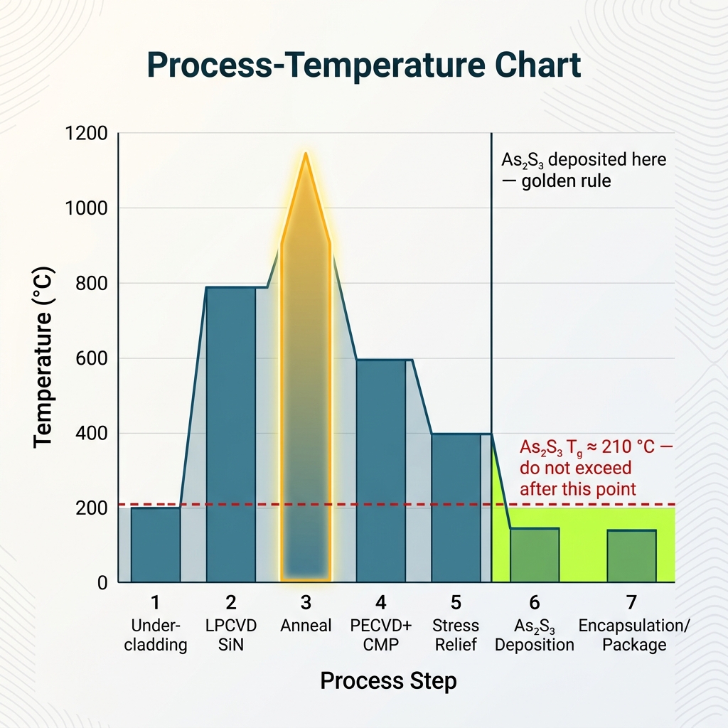 Figure 10
IP-compartmentalized manufacturing
Commodity Si₃N₄ is outsourced to MPW foundries ● LIGENTEC AN350 (200 mm, stoichiometric LPCVD, <0.5 dB/m), with AIM Photonics and imec as backups ● using encrypted / partial GDS so only the non-proprietary nitride layers ever leave the building. Proprietary steps ● the all-optical switch, the As₂S₃ OPC overlay, the stress-relief stack, and hermetic packaging ● stay in-house, both for IP protection and because arsenic cannot enter shared CMOS lines.
Two tracks share one ~$500K budget envelope: a full hybrid MVP (~42 weeks; ~$496K in-house bottoms-up, plus a ~$1M first split-fab tapeout in the seed plan) and a flagship v1 that defers As₂S₃ (~34 weeks; thermo-optic phase trim instead of on-chip OPC) to de-risk first silicon and still demonstrate a 4-qubit GHZ state at >85% fidelity.
Key numbers
Labeled by status so engineering and roadmap stay distinct.
| Parameter | Value | Status |
|---|---|---|
| Operating temperature (core) | 15–45 °C (288–318 K) | Architecture |
| Wavelength | Telecom C-band ~1550 nm | Architecture |
| Backbone loss | ~0.1 dB/cm (claim); 1.77 dB/m thin-core | Claim / demonstrated |
| γ_eff (OPC) | 3–5 (baseline), 8–15 (optimized) W⁻¹m⁻¹ | Claim |
| OPC CW conversion η | 0.5–2% @ 100–200 mW | Model |
| OPC noise floor | <0.01 photons / temporal mode | Target |
| Raman detuning | 7.0–7.8 THz (7.4 THz) | Physics |
| Gate depth (no OPC / with OPC) | 50–100 / 500–1,000+ | Limit / target |
| OPC interval M | 3–20 gates (preferred 10) | Design |
| Switch | TFLN EO sub-ns, >20 dB ext., <0.5 dB IL (committed); ~150–175 fs piezo upgrade | Designed (EO) / verification-pending (piezo) |
| v1 mesh | 8-mode, 28 MZIs, 32 heaters, 16 switches, 16 SPADs | Design |
| SPAD | ≥28% PDE, <20 kHz DCR, <100 ps jitter | Target |
| Homodyne (CV) | 15.3 GHz, Ge p-i-n | Claim |
| Multiplexed delivery | ~97% (K=8, T=4, p=0.1) | Model |
| Footprint | 5 × 5 mm | Design |
What makes this unique
Passive analog correction
No syndrome measurement, no ancillas, no decoder. Correction is a waveguide element, not a protocol.
Room temperature, end to end
Warm-core logic and room-temperature detection ● eliminating both cryogenic SNSPDs (PsiQuantum) and cryogenic PNR arrays (Xanadu). ~99% energy reduction vs. dilution-fridge stacks.
Error bounded by interval, not depth
The Patent 08 result turns depth-limited linear optics into a depth-scalable platform.
One element, every scale
OPC inside the chip (Patent 08), at the source mux (Patent 09), at encoding boundaries (Patent 11), as a built-in calibration probe (Patent 12), across fiber and repeaters (Patent 13), and as a time-reversal simulator (Tier-3).
Dual-use commercial path
Same chip → photonic AI accelerator (near-term revenue) and quantum processor (long-term), de-risking the business.
Confirmed patent white space
No prior art combines OPC + quantum-computing context + periodic multi-point insertion + PIC integration + quantum-grade noise + encoding-aware conjugation.
Control electronics & feed-forward timing
A heralded photonic computer is a race against the photon. Every routing decision must be made and delivered before the photon leaves its delay line.
The feed-forward loop
When an idler photon heralds, a discrete-variable detector fires an avalanche that a custom time-to-digital converter (TDC) timestamps. A field-programmable gate array (FPGA) reads that timestamp, looks up the routing decision in pre-loaded memory, and drives a modulator that triggers the all-optical switch — all while the signal photon waits in an on-chip spiral. In the MVP this is an honest hybrid electronic loop (SPAD → TDC → FPGA → DAC → modulator → switch), not yet a pure all-optical closed loop; femtosecond all-optical feed-forward is a roadmap target.
Two distinct timing regimes coexist and serve different roles:
- Feed-forward gate loop — ~11.2 ns budget. The MBQC fusion path, assuming a pre-calibrated ~30 m external fiber delay and pre-loaded pulse masks.
- Source-multiplexing routing — 20–70 ns. The mux switch-tree decision, with the signal held in a 4–14 m on-chip Si₃N₄ spiral (~1 dB extra loss for a ~10 m line).
Three control tiers run in parallel: an ultra-fast herald engine (<15 ns), a fast thermo-optic mesh-bias loop (~1 ms per full sweep, far too slow for gating — used only for calibration), and a slow supervisory layer (<10 s).
| Stage | Latency |
|---|---|
| SPAD → TDC | 1.0 ns |
| TDC → FPGA (LVDS) | 0.5 ns |
| FPGA sync | 0.5 ns |
| BRAM address + read | 5.0 ns |
| DAC + modulator | 0.7 ns |
| 30 m fiber delay | 6.2 ns |
| Fiber → switch | 0.3 ns |
| Total | ~11.2 ns |
Clock:        100 MHz laser → ×2 → 200 MHz
Coincidence:  |Δt| < 128 ps
TDC bins:     64 ps (fine) / 10 ns (coarse)
Timing jitter:< 0.8 ps RMS (±2 ps guard)
BRAM buffer:  16k frames → 160 µs coverage
FPGA:         Kintex-7 XC7K410T @ 200 MHz
Status: target / design (MVP control-electronics spec). Numbers from internal control-electronics and manufacturing references.
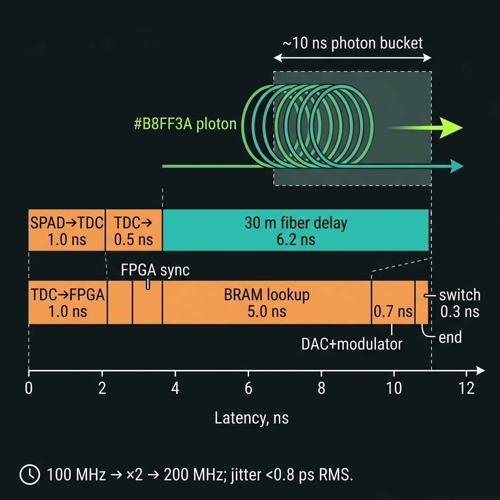 Figure 11
The FPGA — the processor's real-time brain
One reprogrammable chip arbitrates every nanosecond-scale decision on the machine.
A heralded photonic computer is fundamentally a timing machine: photons are produced probabilistically, and the only way to turn that randomness into a deterministic circuit is to detect a herald, decide what to do, and act — all inside the few nanoseconds the partner photon spends in its delay line. No general-purpose processor can meet that deadline. The job falls to a field-programmable gate array (FPGA), a chip whose logic is wired in hardware rather than executed as software instructions. It is the bridge between a high-level circuit description ("apply this unitary, then fuse these two qubits") and the physical layer of analog bias voltages and femtosecond gate triggers on the photonic die.
- Hard determinism. A microcontroller's interrupt latency is tens to hundreds of nanoseconds and varies shot to shot. FPGA logic responds on a fixed clock edge with single-digit-nanosecond, jitter-bounded latency (<0.8 ps RMS) — the photon will not wait for a cache miss.
- True parallelism. Programming 56 thermo-optic heaters, time-stamping 16 detector channels, and arming the switch tree are not queued in sequence — they are physically separate circuits running at the same instant, with no scheduler in between.
- Feed-forward in fabric. The herald→gate decision (detect → look up → fire) is implemented as a short combinational/registered path, hitting a <20 ns target that an instruction-fetch CPU simply cannot reach.
- Reconfigurable. New gate sets, calibration routines, or mesh-programming algorithms ship as a firmware bitstream — no board re-spin. The control plane evolves at the speed of software while keeping the timing of hardware.
Six jobs, running at once
Locked to the laser
The 100 MHz sync output of the mode-locked laser is the master clock. An on-chip MMCM PLL multiplies it ×2 to a 200 MHz fabric clock (clk200, 5 ns period) with <0.5 ps RMS phase noise. Every timing-critical path runs on clk200; the asynchronous LVDS herald is captured through a two-stage synchronizer so the electronics and the photons share one time-base.
Decision in one cycle
A pre-computed routing table lives in dual-port block RAM (16,384 frames × 64 bits). On a herald, the engine forms an address from the coarse time-stamp plus a per-source calibration offset, reads the 64-bit "pulse mask" in a single 200 MHz cycle, and drives it out — 56 switch-control bits + an 8-bit source bus.
Real vs. false heralds
Before acting, the engine validates the event: the firing channel must equal the expected source and the inter-arrival window must satisfy |Δt| < 128 ps. Dark counts and accidentals are rejected in hardware, so the switch only fires on genuine pairs.
Driving the unitary
The FPGA is SPI master to two AD5372 DACs (32 × 16-bit each) that bias the 56 thermo-optic phase heaters of the Clements mesh. A full 56-channel refresh completes in ~54 µs (LDAC-synchronized) — comfortably inside the <100 µs reconfiguration target.
Sub-nanosecond windows
Eight detector-enable outputs use IODELAY primitives for sub-ns placement, with gate widths programmable from 1–100 ns. Gating the SPADs to the expected arrival window suppresses dark counts and afterpulsing without touching the optics.
Stream & correlate
33-bit TDC words (channel + 16-bit coarse + 9-bit fine, 64 ps resolution) are DMA'd into BRAM. The fabric can accumulate coincidence and g²(0) histograms on-chip, while raw time-tags stream to the host over USB-C at ~8 MB/s for tomography.
Inside the herald engine
// fires on every 200 MHz (5 ns) clock edge
on posedge clk200:
  mask_valid <= 0
  if herald_edge:                 // LVDS strobe from TDC
    if  source_id == expected_k   // right SPAD?
    and |Δt_coincidence| < 128 ps:  // genuine pair?
      addr     = coarse_ts
               + offset[source_id]      // per-source delay cal
      mask_out = mask_bram[addr]        // 1-cycle dual-port read
      mask_valid <= 1                    // → DAC → EOM → switch
The whole decision — validate, address, fetch, emit — is bounded by an XDC set_max_delay 4.0 ns constraint from herald_edge to mask_out. The asynchronous detector input is deliberately false_path'd into the synchronizer so the tool closes timing only on the deterministic logic.
Resource budget — Kintex-7 XC7K410T
| Resource | Available | Used |
|---|---|---|
| Logic cells | 406,720 | ~3.7% |
| Block RAM | 28.6 Mbit | ~2% (128 KB masks) |
| DSP48E1 slices | 1,540 | ~1.3% |
| GTX transceivers | 16 | 4 (TDC + DAC) |
| MMCM / PLL | 10 | 1 (100→200 MHz) |
| I/O pins | 500 | ~96 |
The herald engine is tiny — even with a soft CPU and Gigabit Ethernet added, the full control design fits in <50% of a low-cost Artix-7. Headroom is for future gate sets and on-chip correlation, not a present-day bottleneck.
One architecture, three silicon tiers
| Tier | Board / device | Logic cells | Role |
|---|---|---|---|
| Prototype | Digilent Arty A7-100T (Artix-7) | 101k | Bring-up: SPI/DAC, SPAD gating, first feed-forward & HOM measurements |
| Production | AMD KC705 (Kintex-7 XC7K325T) | 326k | FMC DAC daughter-card, GTX transceivers, full 8-mode mesh control |
| Reference spec | Kintex-7 XC7K410T | 407k | Herald-engine timing reference (the budget & XDC above) |
| Roadmap | Zynq UltraScale+ (ARM + FPGA SoC) | — | Folds the supervisory MCU onto the same die; Linux + Python on-chip |
The toolchain is AMD Vivado (Verilog / SystemVerilog with XDC timing constraints); the herald engine, SPI masters, gating logic and DMA are delivered as version-controlled HDL. Honest scope: in the MVP the feed-forward loop is an electronic hybrid (SPAD → TDC → FPGA → DAC → modulator → switch); the ~11.2 ns budget assumes pre-loaded pulse masks and a calibrated external fiber delay, and a pure sub-nanosecond all-optical loop remains a roadmap target. Independent 2026 results on FPGA-driven self-configuring photonic meshes (>98% unitary fidelity) validate that the heavy lifting of mesh programming belongs in exactly this kind of reprogrammable controller.
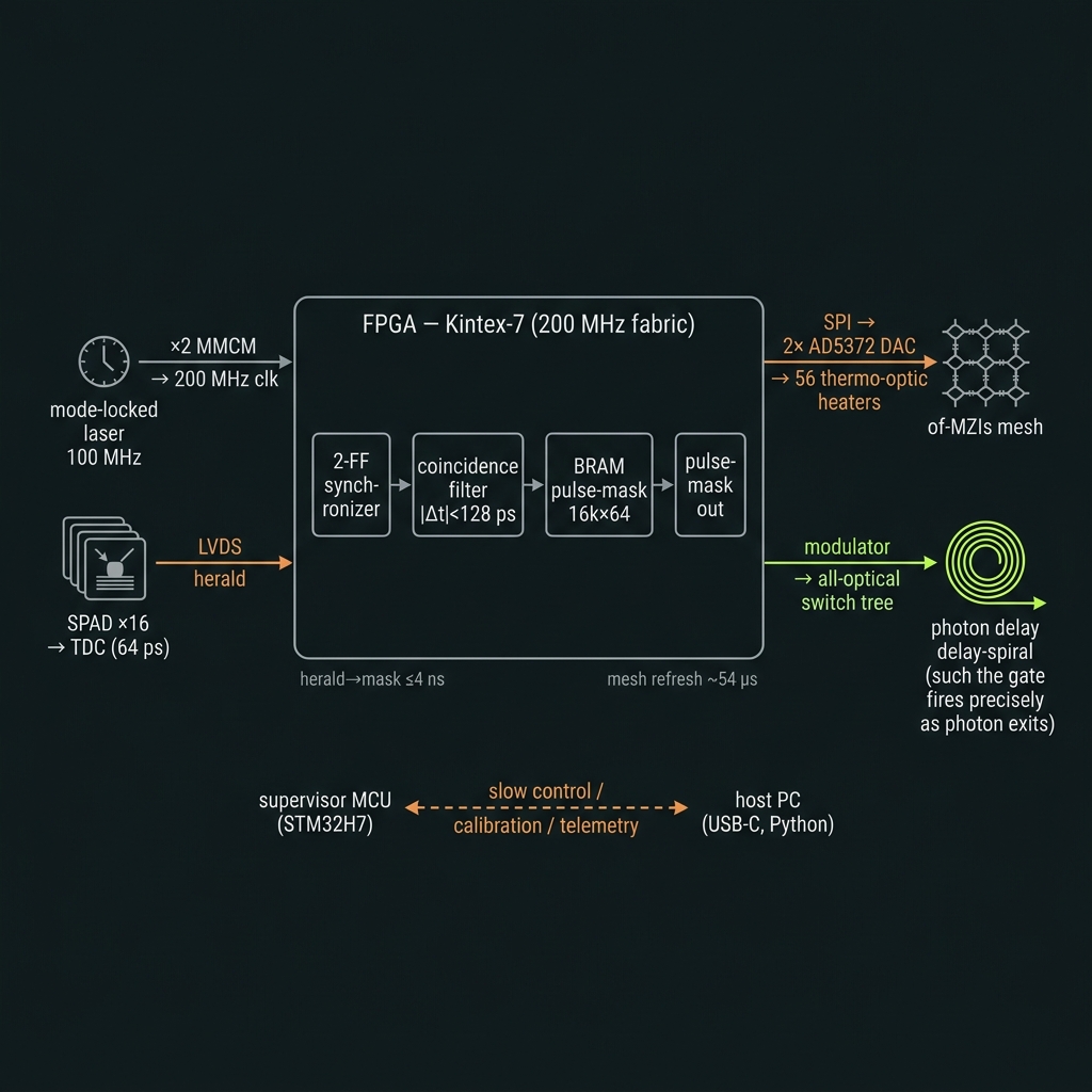 Figure 12
Self-calibration & memory
The same OPC modules that re-tune the chip also refresh stored quantum states — and around them sits a full memory stack, from classical control RAM to roadmap quantum memories.
OPC visibility as a free diagnostic
Every OPC module is already an interferometer. Reading its phase-conjugate visibility directly reports the cumulative phase noise along the path that feeds it:
V = exp(−σ_φ² / 2)
  V = 0.99   → σ_φ ≈ 0.10 rad
  V = 0.999  → σ_φ ≈ 0.045 rad
  V = 0.9999 → σ_φ ≈ 0.014 rad
The module's reflectivity R reports loss non-destructively, and the conjugate's spectral shape reports phase-match drift. Three diagnostics, zero added test structures — versus the 15–20% die area metrology normally consumes.
A chip that re-tunes itself
| Tier | Action | Response |
|---|---|---|
| 1 | Re-optimize nearest phase shifters → max V | <1 ms |
| 2 | Adjust pump power / wavelength | <100 ms |
| 3 | Re-index / reroute around a bad segment | <1 ms (decision) |
| 4 | Permanently isolate segment + alert | days-scale drift |
Post-fabrication calibration targets <60 s (vs ≥45 min for conventional photonic processors), using transfer-learned starting points refined by live OPC-visibility feedback.
How the chip stores memory — classical & quantum
Two very different storage problems live on the same machine.
"Memory" means two completely different things here. Classical memory is ordinary digital storage — the routing tables, calibration constants, and firmware the control electronics need to run the machine; it lives in the FPGA and microcontroller, never on the photonic die. Quantum memory is the genuinely hard problem: holding a photon's fragile quantum state — its phase, superposition, and entanglement — long enough to be useful, without measuring or destroying it. We solve the first with conventional silicon. We approach the second as a tiered stack, from a simple on-chip delay line you can build today to matter-based memories on the roadmap, all sharing one trick: an OPC pass at readout that reverses the dephasing accrued while the state sat in storage.
Photon pairs are born probabilistically — you cannot demand one on command. The entire architecture is a scheme for turning that randomness into a deterministic circuit, and every step needs to hold a photon still while classical electronics catch up:
- Feed-forward (~10 ns). A measurement result must steer a partner photon that is still in flight — it waits in a delay spiral for the ~11.2 ns herald-to-gate loop.
- Source multiplexing (20–70 ns). A heralded photon is parked in a 4–14 m spiral while the switch tree decides where to route it.
- Multi-pass / iterative algorithms. Deep or repeated circuits (e.g. Grover) reuse the same hardware many times — the photon must survive each loop.
- Repeaters (hundreds of µs – ms). A node must hold one half of an entangled pair until its partner arrives over tens of km of fiber.
1 · Classical memory — the control plane
The photonic chip itself holds no electronic bits. All classical state lives in three tiers of conventional silicon that surround it — fast FPGA fabric for nanosecond decisions, a supervisory microcontroller for secure boot and calibration, and the host PC for data and configuration files.
Decisions in hardware
The critical store is a 128 KB dual-port block RAM (16,384 frames × 64 bits) holding pre-computed routing pulse masks — a 160 µs ring buffer read in a single 200 MHz cycle on each herald. Additional fabric RAM (~120 Kb) carries the TDC time-tag DMA buffer, on-chip coincidence/g²(0) histograms, and the phase→voltage heater calibration LUT.
Boot, keys & calibration
An STM32H7 holds firmware in two 1 MB flash banks (secure bootloader + failsafe backup image), per-device calibration in 512 KB AXI SRAM, signing/encryption keys in a 64-byte one-time-programmable block, and a monotonic anti-rollback counter in 4 KB battery-backed SRAM.
Data & config files
The host streams raw 64 ps time-tags to HDF5 at ~8 MB/s for tomography, and generates the configuration the chip boots from: pulse_masks.npy (the 128 KB mask array), control_map.csv (per-source delay offsets), and spad_cal.csv (per-heater Vπ and DAC trim).
| Store | Capacity | What it holds | Persistence |
|---|---|---|---|
| FPGA pulse-mask BRAM | 128 KB (16,384 × 64-bit) | Pre-computed feed-forward routing masks | Volatile (loaded at boot) |
| FPGA fabric BRAM (other) | ~120 Kb | TDC DMA buffer, coincidence/g²(0) histograms, phase→V cal LUT | Volatile |
| Board DRAM | 256 MB – 1 GB DDR3 | Soft-CPU / Ethernet stacks & buffers | Volatile |
| Config flash | 16 MB QSPI | FPGA bitstream | Non-volatile |
| MCU flash | 2 × 1 MB banks | Secure bootloader + application + backup image | Non-volatile |
| MCU OTP | 64 bytes | ED25519 public key + AES-256 key | One-time, unreadable |
| MCU backup SRAM | 4 KB | Monotonic firmware version counter | Battery-backed |
| MCU working RAM | 128 KB DTCM + 512 KB AXI | Calibration tables, mask staging buffer | Volatile |
| Host archive | HDF5 on disk | Raw time-tags, tomography datasets | Persistent |
Status: all control-electronics figures are MVP design/target (control-electronics & manufacturing spec). The reference FPGA is a Kintex-7; the prototype runs on a low-cost Artix-7 board. No firmware or calibration files are fabricated yet.
2 · Quantum memory — storing the photon's state
You cannot copy a qubit and you cannot read it without collapsing it, so quantum memory must hold the state physically and hand it back intact. We treat this as a ladder of mechanisms with increasing hold time and increasing maturity — the bottom rung ships in v1, the upper rungs are roadmap. The unifying idea is that OPC refresh decouples coherence from time: whatever dephasing builds up during storage is phase-conjugated away at readout, so the error is bounded by the refresh interval, not the total hold time — leaving loss, not dephasing, as the real limit.
Delay spirals
A photon is simply kept moving in a Si₃N₄ waveguide loop. At a group index ≈2.0 light travels ~6.7 ns per metre, so a ~2 m spiral buys the ~10 ns feed-forward bucket and a 4–14 m spiral the 20–70 ns mux window (~1 dB loss per ~10 m). Passive and non-refreshing — longer holds simply cost more loss.
Time-bin recirculation
A fast switch diverts the photon into a loop containing a single OPC module; every round trip applies one round of phase refresh, so coherence no longer decays pass-by-pass. One OPC module serves all passes — ideal for multi-pass and iterative algorithms. The ceiling becomes loss (~3 dB per OPC pass), not dephasing.
Phononic (SBS) buffer
The photon is written into a long-lived acoustic phonon in As₂S₃ via stimulated Brillouin scattering (ΩB ≈ 7.7 GHz, lifetime ~5–50 ns) and read back out with an OPC phase-conjugate pulse. It is the same physics we deliberately suppress in the OPC pumps, so a memory build needs a dedicated or dual-function chalcogenide section.
Rare-earth atomic memory
A telecom photon is mapped into the long-lived coherence of erbium ions (Er:YSO) and recalled on demand — externally demonstrated at µs–ms storage with multimode capacity (≈20 temporal + 3 spectral modes). Telecom wavelength keeps it native to our C-band stack; best coherence may require a locally cooled module.
SiC spin register
The most durable rung: a photonic state is stored in silicon-vacancy electron–nuclear spins in isotopically purified 4H-SiC, evanescently coupled to the Si₃N₄ bus. Literature shows T₂ > 1.5 ms at 300 K under dynamical decoupling — a true on-demand matter memory for feed-forward buffering and repeater nodes.
OPC refresh
Across every rung, a phase-conjugate pass at readout reverses storage-interval dephasing — a Loschmidt echo in hardware. That is what lets a ms-class spin or a recirculating loop stay coherent far longer than a passive store of the same length.
The math behind "refresh, don't decay"
Passive store (no refresh):
   V(t) = exp(−σ² · t/τ_seg / 2)   → decays

With OPC refresh every interval M:
   V∞ ≤ M·σ² / η                   → bounded, flat
        (σ = phase error/segment,
         η = OPC conversion eff.)

Multi-pass recirculation:
   η_eff = 1 − (1−η)^K_loop
        (e.g. η=1%, K=10 → ~9.6%)

Hard limit once phase is handled:
   loss ≈ 3 dB per OPC pass
Quantum-memory stack at a glance
| Layer | Hold time | Status |
|---|---|---|
| Delay spirals (Si₃N₄) | 20–70 ns (≥10 ns FF) | Baseline / v1 |
| Time-bin recirculation + OPC | Multi-pass | Near-term (Tier-2) |
| Phononic (SBS) buffer | 5–50 ns (~10 ns ext.) | Roadmap (Tier-3) |
| Rare-earth (Er:YSO) | µs–ms (ext.) | Roadmap (Tier-3) |
| SiC spin register | ms-class T₂ | Roadmap (P1) |
µs–ms and ~10 ns hold times are external literature benchmarks, not QLT-fabricated results. v1 ships delay spirals only; single-photon OPC in an integrated waveguide is our #1 validation milestone, and every advanced rung depends on it.
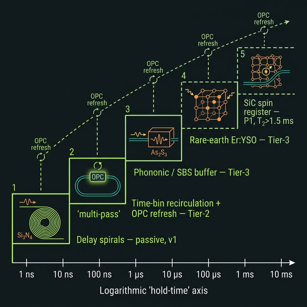 Figure 13
Networking, interconnects & scaling
OPC is mid-span spectral inversion — the same trick that compensates dispersion in classical long-haul fiber — extended to single photons (Patent 13).
Distance tiers
| Scale | Range | Limiting problem |
|---|---|---|
| Intra-rack / board | <1 m | phase stability |
| Data-center links | 0.1–100 m | indistinguishability |
| Metropolitan | 1–50 km | dispersion + phase drift |
| Direct fiber | to ~100 km | loss (~20 dB, ~1% survival) |
| Regional (repeaters) | 150–400 km | requires entanglement swap |
What OPC fixes: a mid-span conjugation makes the second symmetric span cancel even-order chromatic dispersion (β₂, β₄…) — e.g. the ~850 ps of broadening a 1 nm photon picks up over 50 km of SMF-28 (17 ps/nm/km). What it does not fully fix: odd-order dispersion (β₃) and stochastic polarization-mode dispersion, which only cancel for symmetric fiber.
A room-temperature OPC repeater node — dual OPC inputs, a quantum-memory buffer, and a Bell-state measurement — draws on the order of ~15 W, versus 450–3,200 W for cryogenic alternatives.
| Fiber CD (SMF-28) | ~17 ps/(nm·km) |
| Pump per node | 50–150 mW CW |
| Module insertion loss | 3–5 dB (target) |
| PON branches | ≥64 (AWG) |
| Remote-node stabilization power | 0 W (passive) |
Single-photon OPC through fiber is theoretically supported (Gaeta & Boyd 1995) but not yet experimentally demonstrated; fidelity tables are patent claims, not lab data. Chiplet/backplane and global-internet tiers are roadmap.
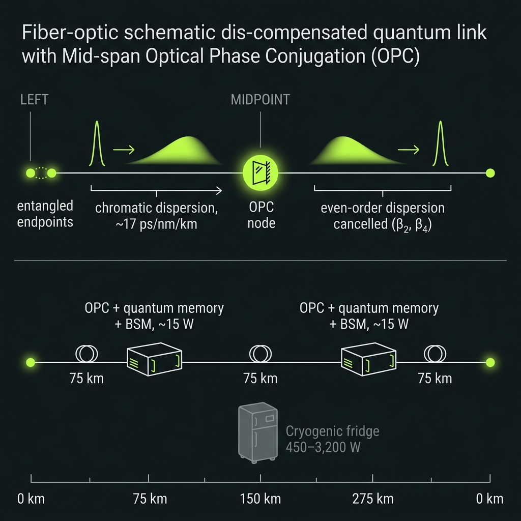 Figure 14
Status, provenance & honest caveats
This page is unredacted on purpose. Here is the clean separation between what ships in v1, what is a design target, and what is roadmap — plus the open questions we are still validating.
- Bench Type-II ppKTP SPDC source (775→1550 nm)
- Foundry Si₃N₄ photonics (LIGENTEC AN350, split-fab)
- 8-mode Clements mesh: 28 MZIs, 32 thermo-optic heaters
- Room-temperature GeSi SPAD readout + FPGA feed-forward
- Thermo-optic phase trim (As₂S₃ OPC deferred to de-risk)
- Target demo: 4-qubit GHZ state, >85% fidelity
- On-chip SFWM micro-ring sources (production)
- On-chip As₂S₃ OPC overlay (Patent 10 process)
- 500–1,000+ gate depth via periodic OPC lattice
- Qudit / high-dimensional frequency-bin encoding
- Phononic / rare-earth / spin quantum memory
- Fiber repeaters and rack-scale OPC interconnects
The open questions we are still validating
- Single-photon OPC coherence preservation is our #1 experimental milestone. The physics (Gaeta & Boyd 1995) supports it for quadrature-squeezed light, but it has not yet been demonstrated for single photons in an integrated waveguide.
- Conversion efficiency η. CW OPC at our baseline (0.5–2% at 100–200 mW) is not enough to reach the headline 1,000-gate depth on its own. That target assumes pulsed/resonant pumping (higher η) and a recirculating geometry.
- Geometry precondition. The error-bounding math is rigorous when the conjugate re-traverses the same static errors — i.e. recirculating or symmetric layouts. A purely forward "lattice" of independent random gate errors is not fully cancelled by conjugation alone.
- Loss tax. Each OPC pass costs ~3 dB, so the lattice is loss-limited until per-module loss drops toward ~1 dB; correction density must be balanced against photon survival.
- What OPC does not do. It corrects coherent phase / dephasing only — not photon loss, bit-flips, or depolarizing errors. It is a passive analog pre-layer that lowers the phase-error rate seen by digital QEC (surface / LDPC / GKP); it complements those codes, it does not replace them. In patent language this is "error mitigation," not full fault-tolerant QEC.
- Switch maturity. The ~150–175 fs / >30 dB / <0.5 dB switch figures are cited from the licensable device family and remain verification-pending; the patent claims are written technology-agnostically (electro-optic / Kerr / MEMS fallbacks) rather than depending on one mechanism.
Every figure on this page is traceable to the internal corpus — the Final Revised patent specifications, the engineering whitepaper, and the MVP manufacturing references — cross-checked by 25 parallel research passes and graded demonstrated / target / claim. The key external anchors:
- Collins et al., Opt. Lett. 37, 3393 (2012) — As₂S₃ low-Raman window at 7.4 THz.
- Bose et al., Light: Sci. Appl. 13, 156 (2024) — anneal-free deuterated Si₃N₄ at 1.77 dB/m (0.177 dB/cm).
- Gaeta & Boyd (1995) — FWM phase conjugation preserves quadrature squeezing.
- PsiQuantum (Nature, 2025) — 99.22% same-chip fusion fidelity (benchmark for the gate model).
From architecture to industrial hardware
See the foundry-to-package manufacturing path, the patent portfolio that protects it, and the full product specification.