QUASAR SUPER — complete fabrication process
Start-to-finish manufacturing traveler for GF(128) on the QLT 200 mm Si₃N₄ / TFLN / As₂S₃ platform. 128 channels · Δf = 35 GHz · B_comb = 4.45 THz · Region II. Every thin-film layer with method, temperature, timing, and thickness — plus metrology gates and yield techniques for correctly printed gates.
Eight steps — wafer to tested die
Tap any step. Golden rule: no process >210 °C after As₂S₃ deposition.
SUPER fabrication steps
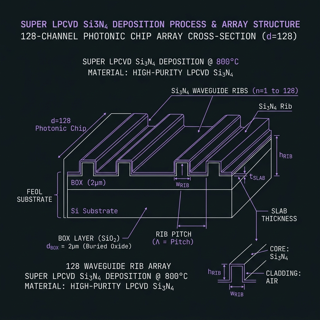
FEOL → bond → BEOL → testSubstrate & LPCVD Si₃N₄
→Wafer QC → thermal BOX 1000 °C → LPCVD Si₃N₄ 800 °C, 300–400 nm
Equipment: View equipment spec · research
How we do it: Sign traveler gate before releasing lot to next step; duplicate monitor wafer per batch.
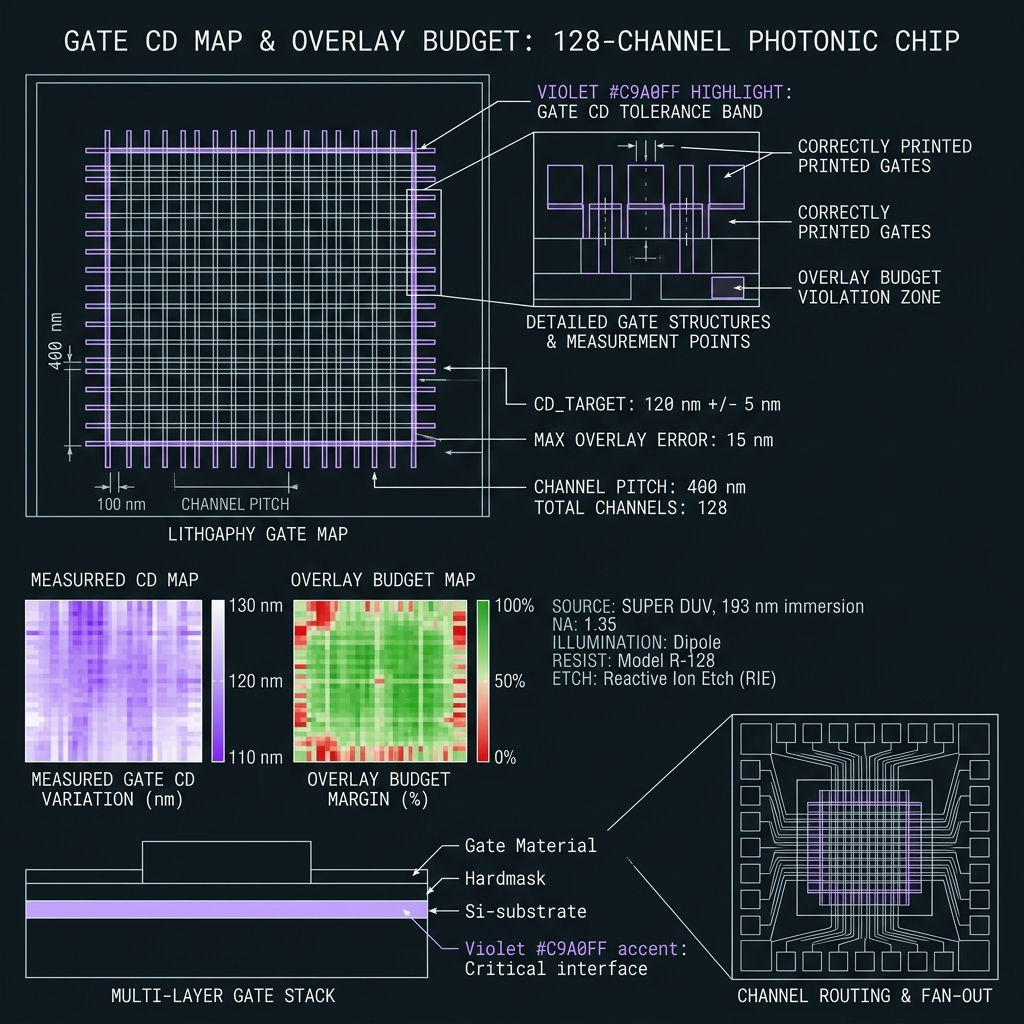
Lithography & gate patterning
→DUV 193 nm; CD σ/μ <3%; OPC monitor structures for correctly printed gates
Equipment: View equipment spec · research
How we do it: Sign traveler gate before releasing lot to next step; duplicate monitor wafer per batch.
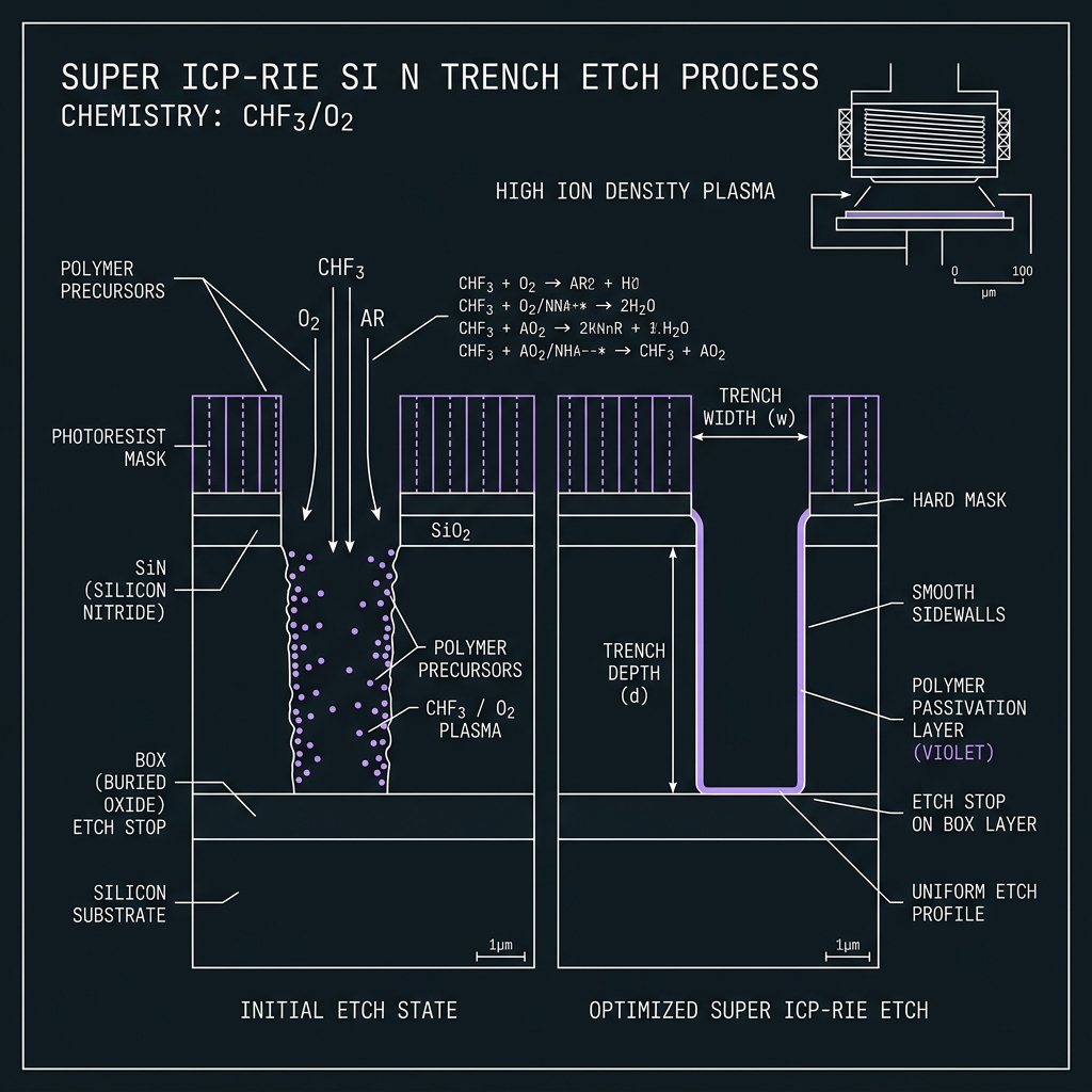
ICP-RIE etch
→CHF₃/O₂ ICP; sidewall RMS <5 nm; etch-stop on BOX
Equipment: View equipment spec · research
How we do it: Sign traveler gate before releasing lot to next step; duplicate monitor wafer per batch.
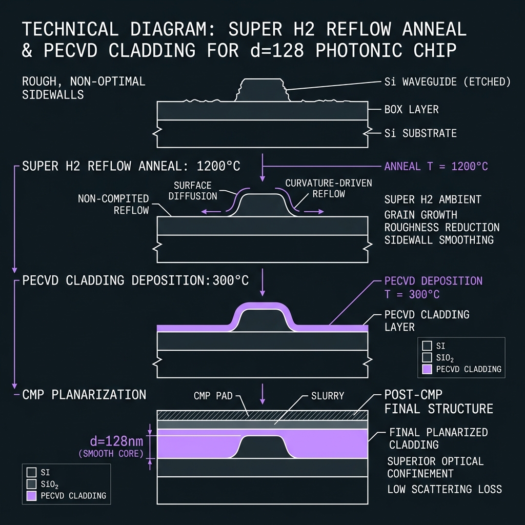
Anneal, clad & CMP
→H₂ reflow 1150–1250 °C → PECVD SiO₂ 300 °C → CMP planarization
Equipment: View equipment spec · research
How we do it: Sign traveler gate before releasing lot to next step; duplicate monitor wafer per batch.
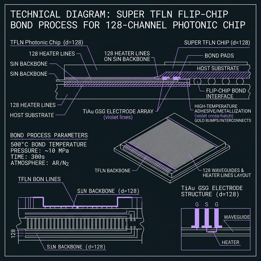
TFLN bond & metallization
→Ion-cut bond ≤500 °C; Ti/Au GSG ≤250 °C; heater routing
Equipment: View equipment spec · research
How we do it: Sign traveler gate before releasing lot to next step; duplicate monitor wafer per batch.
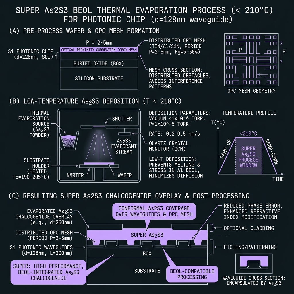
As₂S₃ BEOL overlay
→Thermal evaporation <210 °C; Raman stoichiometry gate; golden rule enforced
Equipment: View equipment spec · research
How we do it: Sign traveler gate before releasing lot to next step; duplicate monitor wafer per batch.
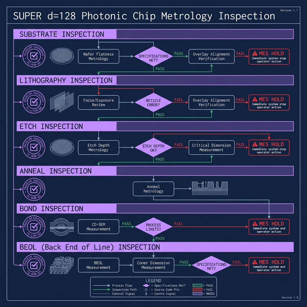
Metrology hold
→Ellipsometry, CD SEM, IL witness — go/no-go before dice
Equipment: View equipment spec · research
How we do it: Sign traveler gate before releasing lot to next step; duplicate monitor wafer per batch.
Dice, package & test
→Dicing → fiber attach → wafer-level quantum test
Equipment: View equipment spec · research
How we do it: Sign traveler gate before releasing lot to next step; duplicate monitor wafer per batch.
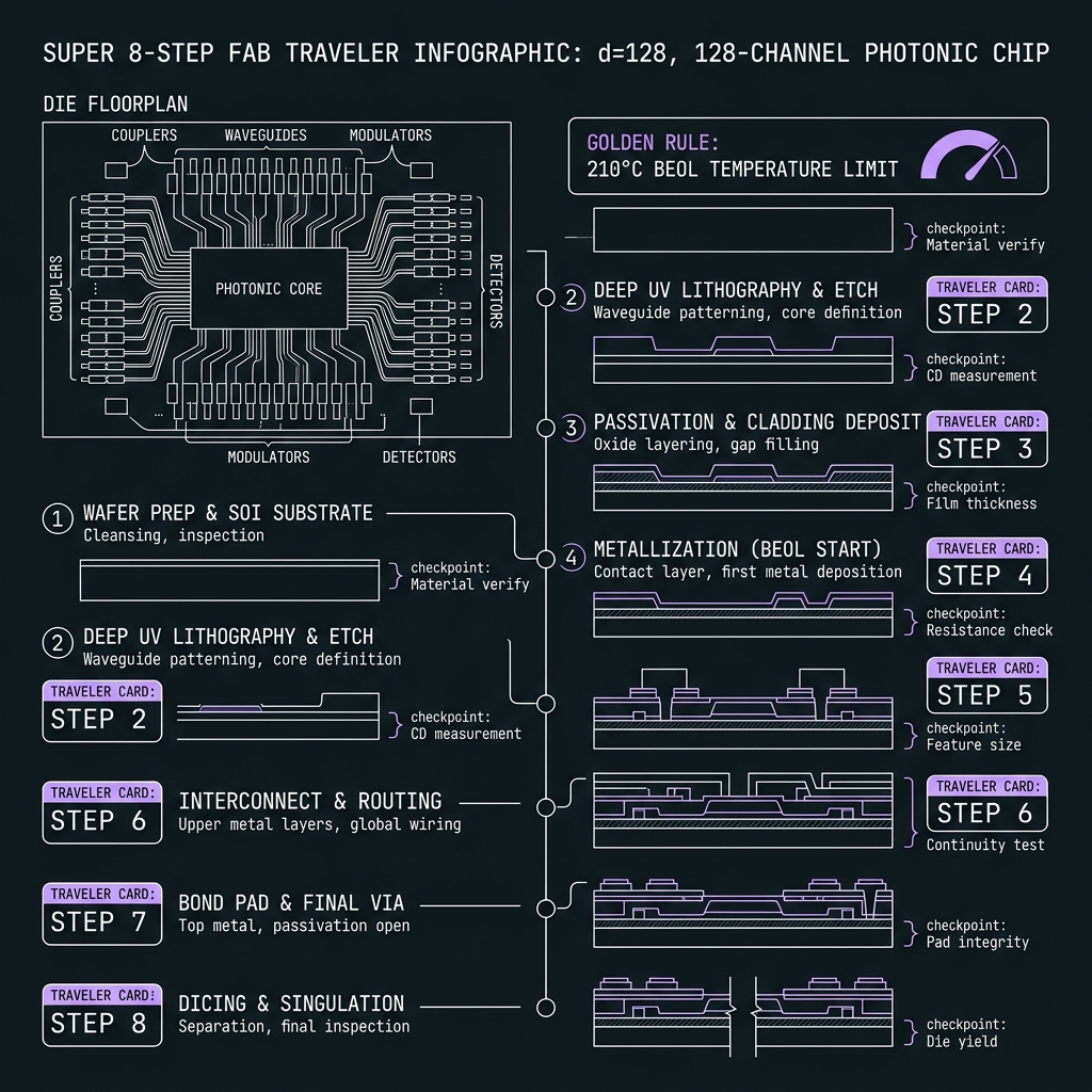 Figure 1
Deposition order — method, temp, time, thickness
| Layer | Material | Method | Temp | Time | Thickness |
|---|---|---|---|---|---|
| L0 | Si handle | Incoming QC | — | — | 200 mm |
| L1 | Thermal BOX | Wet O₂ / furnace | 1000 °C | 4–8 h | 2 µm |
| L2 | LPCVD Si₃N₄ | DCS+NH₃ | 800 °C | 45–90 min | 300–400 nm |
| L3 | DUV resist | 193 nm spin | 23 °C | 60 s | 200 nm |
| L4 | SiN etch | ICP-RIE | RT | 3–8 min | full |
| L5 | H₂ reflow | Furnace H₂ | 1150–1250 °C | 2–6 h | — |
| L6 | PECVD clad | SiH₄+N₂O | 300 °C | 10–20 min | 1.5–2 µm |
| L7 | CMP | Slurry polish | RT | 5–15 min | planar |
| L8 | TFLN bond | Ion-cut | ≤500 °C | 2–4 h | 300–600 nm |
| L9 | Ti/Au GSG | E-beam + lift-off | ≤250 °C | 30–60 min | 200/500 nm |
| L10 | As₂S₃ OPC | Thermal evap | <210 °C | 20–40 min | 0.5–2 µm |
SUPER delta: 128 active channels · calibration pairs N(N−1) = 16,256 · SUPER chip reference
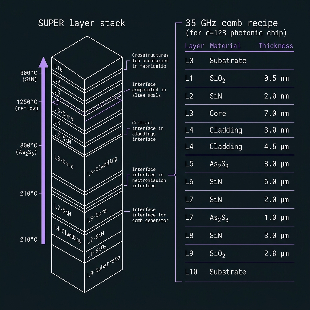 Figure 2
Front-end through BEOL
LPCVD Si₃N₄ @ 800 °C
DCS+NH₃, 45–90 min, 300–400 nm. Stress map gate ±150 MPa. LPCVD furnace.
Correctly printed gates
CD σ/μ <3%; overlay ≤50 nm scaling. OPC monitor bars per reticle. DUV scanner.
H₂ reflow + PECVD
1150–1250 °C reflow; 300 °C PECVD clad; CMP planar. Anneal furnace.
Go/no-go gates at every step
- Post-LPCVD: ellipsometry thickness ±3% · stress window
- Post-litho: CD SEM σ/μ <3% on gate arrays
- Post-etch: SEM sidewall RMS <5 nm
- Post-bond: modulator IL <0.5 dB
- Post-As₂S₃: Raman stoichiometry ±2%
- Pre-dice: full PIC test — hold lot on fail
MES barcode lockout prevents golden-rule violations. Independent QA sign-off required. research
Figure 3Maximizing correctly printed gates
Directed calibration pairs N(N−1) = 16,256. Wafer scatter 5–15% accepted — recovered by ChiL self-calibration (~10 iterations, O(kN)→O(1)) rather than scrap.
- SPC on CD, IL, crosstalk per equipment fleet
- Octet tiling for independent yield islands @ d≥16
- Redundant gate copies on critical paths (GEMINI-class)
- Thermal crosstalk eigenbasis decorrelation before per-tooth trim
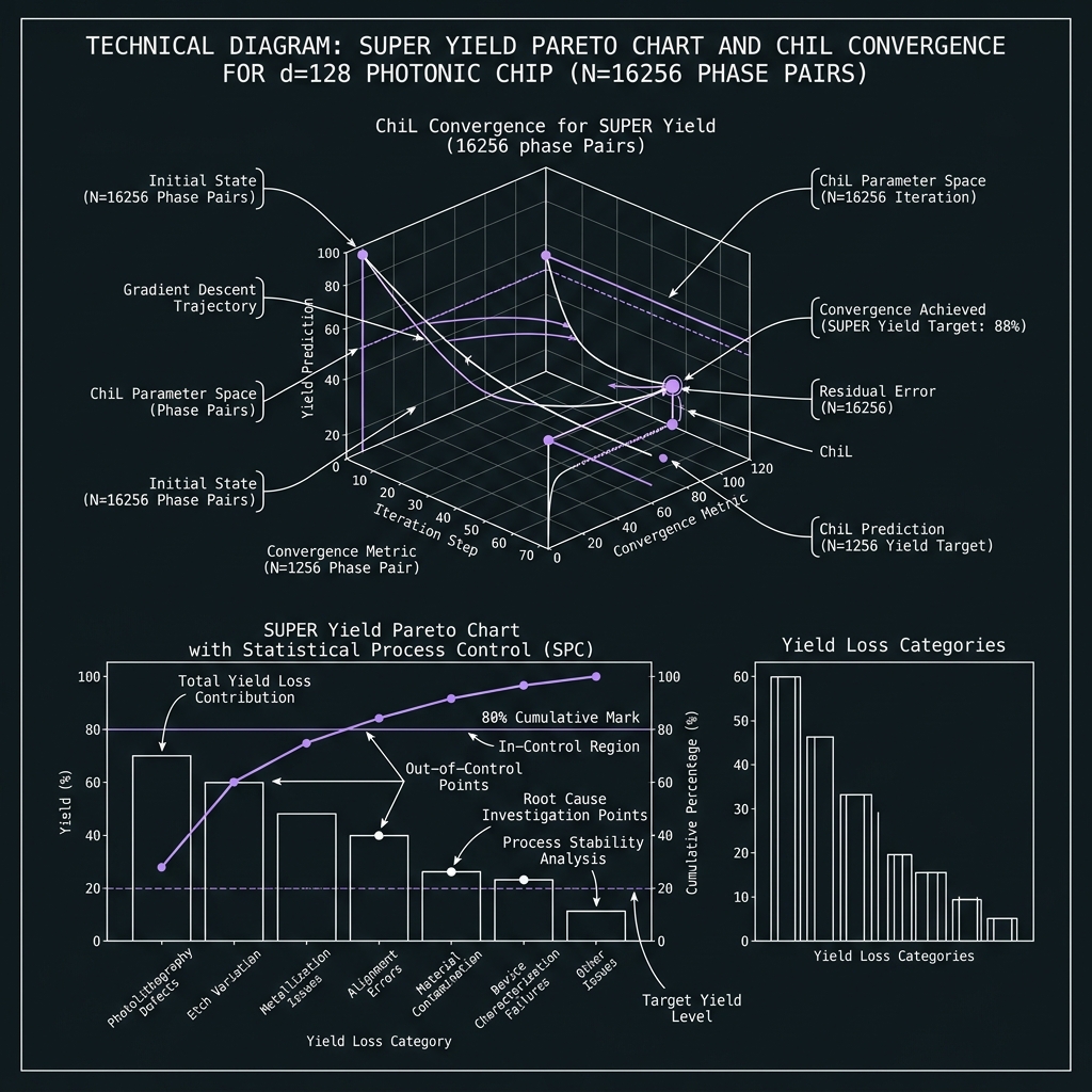 Figure 4