Stress-Relief Cladding for Hybrid Waveguides
A multi-layered cladding architecture that solves the mechanical reliability problem of combining dissimilar materials on a photonic chip — enabling crack-free, quantum-grade hybrid waveguides that survive industrial thermal cycling from −40°C to +85°C.
CTE mismatch destroys hybrid photonic waveguides
Combining silicon nitride (CTE 3.0×10⁻⁶/K) with chalcogenide overlays like As₂S₃ (CTE 21.6×10⁻⁶/K) creates a 7× thermal expansion mismatch. During fabrication cooldown from deposition temperatures, this mismatch generates interfacial shear stress of 20–50 MPa — exceeding defect nucleation thresholds at pre-existing sidewall roughness sites. The result: spontaneous micro-crack formation that propagates across the wafer, destroying the phase-conjugate wavefront integrity required for quantum-grade OPC.
Five-structure hierarchical stress management
A graded-CTE cladding stack (SiON intermediate at 5–8×10⁻⁶/K), patterned stress-isolation trenches (2–5 µm width, >20 µm from waveguide), compliant BCB polymer interlayer (Young's modulus 2.9 GPa), segmented chalcogenide overlays (0.5–2 mm segments with adiabatic tapers), and ALD conformal adhesion layers (10–50 nm SiO₂/Al₂O₃) — working in concert to reduce interfacial strain from 20–50 MPa to below 0.5 MPa while maintaining sub-nanometer surface roughness at all interfaces.
System overview
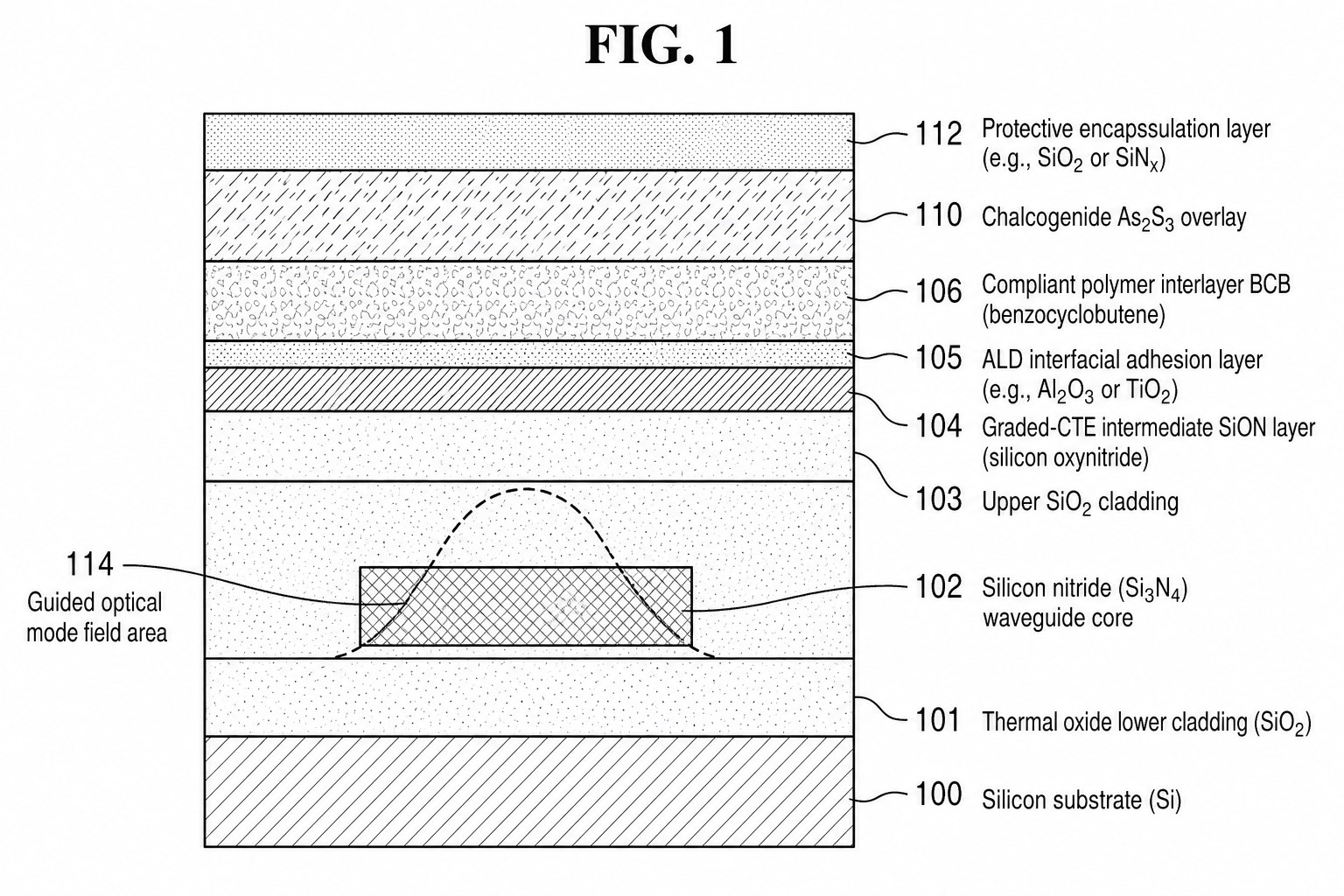
FIG. 1 — Cross-sectional view of stress-relieved hybrid waveguide structure showing the multilayer graded-CTE cladding stack, Si₃N₄ core, and chalcogenide overlay
Graded-CTE Architecture (102–110)
The Si₃N₄ core (102) is encapsulated by a graded-CTE SiON intermediate layer (104) with refractive index 1.55–1.80, an ALD adhesion layer (105) of 10–50 nm conformal SiO₂ or Al₂O₃, and a compliant BCB polymer interlayer (106) at 1–5 µm thickness. The As₂S₃ overlay (110) sits atop this engineered stack, ensuring no single interface experiences a CTE ratio exceeding 3:1.
Stress-Isolation Trenches & Segmentation
Patterned trenches (2–10 µm wide) etched through the SiO₂ cladding to the silicon substrate create stress-isolated islands, arresting crack propagation while maintaining >20 µm separation from waveguides to preserve evanescent field integrity. The As₂S₃ overlay is segmented into 0.5–2 mm sections with 2–5 µm gaps and adiabatic tapers (<0.01 dB loss per gap), allowing independent thermal expansion of each segment.
Key performance parameters
| Parameter | Specification | Significance |
|---|---|---|
| Si₃N₄ Core CTE | 3.0 × 10⁻⁶ /K | Baseline low-expansion waveguide material |
| As₂S₃ Overlay CTE | 21.6 × 10⁻⁶ /K | High-nonlinearity material with 7× CTE mismatch |
| Graded SiON CTE | 5–8 × 10⁻⁶ /K | Intermediate layer reduces per-interface CTE ratio to <3:1 |
| BCB Young's Modulus | 2.9 GPa | 24× more compliant than SiO₂ (70 GPa) for strain absorption |
| ALD Adhesion Layer | 10–50 nm (SiO₂ / Al₂O₃) | Conformal coverage, diffusion barrier, sub-nm surface smoothing |
| Stress-Isolation Trench Width | 2–5 µm | Arrests crack propagation; positioned >20 µm from waveguide |
| Interfacial Strain (mitigated) | <0.5 MPa | Reduced from 20–50 MPa baseline — below failure threshold |
| Surface Roughness | <0.8 nm RMS | Preserves phase-conjugate wavefront at all interfaces |
| Thermal Cycling Range | −40°C to +85°C | Full industrial qualification without degradation |
| Fabrication Yield Improvement | <30% → >80% | Eliminates cracking as primary yield failure mode |
Why this matters
Crack-Free Operation
Interfacial strain reduced from 20–50 MPa to below 0.5 MPa — well below the critical failure stress of the Si₃N₄/As₂S₃ stack. Zero crack propagation through 1000+ thermal cycles at full industrial qualification range (−40°C to +85°C).
Sub-nm Surface Roughness
Surface roughness maintained below 0.8 nm RMS at all interfaces including the BCB/As₂S₃ boundary. Spin-coated BCB achieves <0.5 nm inherent roughness — critical because interface roughness is the dominant scattering loss mechanism for the backward-propagating conjugate wave.
−40°C to +85°C Qualification
Meets Telcordia GR-468 and MIL-STD-883 industrial temperature qualification. Segmented overlay design allows each 0.5–2 mm section to expand independently, preventing longitudinal stress accumulation across the full waveguide spiral length.
CMOS Back-End Compatible
All five cladding structures deposited below 300°C. BCB cured at <250°C, As₂S₃ deposited at <200°C (below its Tg ≈ 200°C), ALD at 150–250°C. Compatible with standard 200 mm/300 mm wafer processing at commercial photonic foundries.
30% → 80%+ Wafer Yield
Film cracking is the #1 yield failure in hybrid photonic integration for Si₃N₄ cores >400 nm with chalcogenide overlays. Eliminating it transforms economics from research-grade single-device fabrication to volume manufacturing with commercial yield targets.
Five Independent Mechanisms
Graded CTE, isolation trenches, compliant interlayer, segmented overlay, and ALD adhesion provide redundant protection. Any single mechanism failing does not compromise the waveguide — the remaining four maintain structural integrity and optical performance.
Built on established science
Standard Semiconductor Technique
Graded coefficient-of-thermal-expansion interlayers are used throughout the semiconductor industry for bonding dissimilar materials — from silicon-on-insulator wafers to III-V integration. PECVD SiON with tunable O₂/N₂ ratios achieves precise CTE targeting at 5–8×10⁻⁶/K.
Proven in MEMS & Photonics
Etched stress-isolation trenches are well-established in MEMS and photonic ICs. Luke et al. (Optics Express 2013) demonstrated Q factors of 7×10⁶ using isolation trenches; Epping et al. (2015) achieved crack-free 900 nm Si₃N₄ via damascene process with trench confinement.
Atomic Layer Deposition
ALD-deposited SiO₂/Al₂O₃ with angstrom-level thickness control (10–50 nm) provides conformal coverage, chemical adhesion, arsenic/sulfur diffusion barrier, and sub-nanometer surface smoothing — routinely used in semiconductor manufacturing for interface engineering.
Benzocyclobutene (Cyclotene)
BCB is commercially available (Dow Cyclotene 3022-46), with verified properties: Young's modulus 2.9 GPa, optical loss <0.5 dB/cm at 1550 nm, Tg ≈ 350°C after full cure, surface roughness <0.5 nm RMS when spin-coated. Widely used in photonic packaging.
Connected patent architecture
Self-Phase-Matched Hybrid Nonlinear Waveguide
Patent 04 provides the mechanical reliability layer that transforms Patent 02's Si₃N₄/As₂S₃ hybrid OPC waveguide from a lab demonstration into a manufacturable product surviving industrial thermal cycling.
View Patent →Acoustic Phonon Suppression in Hybrid Waveguides
The compliant BCB interlayer and stress-isolation trenches complement Patent 10's acoustic suppression by mechanically decoupling the waveguide from substrate phonon modes.
View Patent →Room-Temperature Photonic Quantum Processor
The processor architecture (Patent 01) requires crack-free hybrid waveguides for its OPC modules. Patent 04's stress relief enables the full processor to be fabricated on a single chip without mechanical failure.
View Patent →Enabling reliable manufacturing at scale
This patent transforms Patent 02's waveguide from a lab demonstration to a manufacturable product. Without stress-relief cladding, hybrid waveguides crack during thermal cycling — with it, they survive industrial qualification and achieve >80% wafer yield, unlocking volume production of quantum photonic processors.