Self-Phase-Matched Coherence-Restoration Waveguide
The optical engine at the heart of QLT's phase-correction architecture — a hybrid nonlinear waveguide that reverses quantum decoherence passively via four-wave mixing, with no active electronics and no cryogenics.
Optical phase errors destroy quantum information
Every waveguide, splitter, and coupler introduces phase shifts from manufacturing imperfections, thermo-optic drift (dn/dT), and material dispersion. In monolithic Si₃N₄, these errors accumulate linearly with circuit depth. After ~50–100 operations, quantum visibility collapses — an impenetrable "coherence wall." Monolithic Si₃N₄ provides only γ = 0.3–1.2 W⁻¹m⁻¹, requiring multi-centimeter paths that worsen the problem. Silicon waveguides suffer fatal two-photon absorption at telecom wavelengths (1.12 eV bandgap).
Hybrid localized-overlay architecture for quantum-grade OPC
A monolithic hybrid PIC pairs a stoichiometric Si₃N₄ foundational core (5.0 eV bandgap — no TPA) with localized As₂S₃ chalcogenide overlays that boost γ_eff to 10–12 W⁻¹m⁻¹. Adiabatic mode converters transition between regions with <0.2 dB loss. The cascaded spiral geometry provides self-phase-matching across 300 nm bandwidth while geometrically filtering spontaneous noise. Raman scattering is suppressed to <0.01 photons/mode at 7.4 THz detuning — enabling quantum-grade operation at room temperature.
System overview
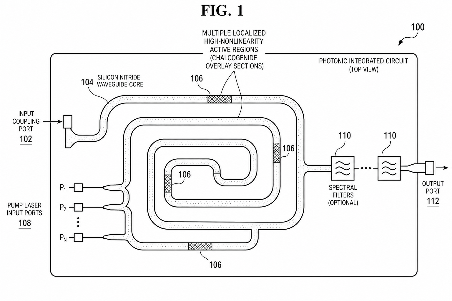
FIG. 1 — Top-down schematic of the photonic integrated circuit showing the foundational Si₃N₄ core arranged in a cascaded multi-segment spiral geometry (23 segments) with localized high-nonlinearity As₂S₃ chalcogenide active regions (OPC nodes) and input/output coupling ports.
Si₃N₄ Core + As₂S₃ Chalcogenide Overlay
The foundational Si₃N₄ core (800 nm × 400 nm cross-section) provides the ultra-low-loss propagation path (<0.1 dB/cm). Localized As₂S₃ chalcogenide overlay regions (500 nm thick) are deposited only on designated nonlinear segments, boosting γ_eff to 10–12 W⁻¹m⁻¹ while preventing cumulative stress and propagation loss. The cascaded geometry packs >12.4 cm interaction length within a 5 mm × 5 mm footprint.
Adiabatic Mode Conversion + Raman-Silent Window
400 μm adiabatic mode converters with 300 nm-precision sub-wavelength tapers transition between core and overlay regions at <0.2 dB per transition. Pump-signal detuning is constrained to a 7.4 THz Raman-silent window (6.5–8.5 THz), suppressing spontaneous Raman scattering to <0.01 photons/temporal mode — three orders of magnitude below the quantum-grade threshold.
Why this matters
Ultra-Low Noise
Spontaneous Raman noise suppressed to <0.01 photons/temporal mode at 300K. Multi-photon generation probability <0.01%. Spontaneous emission maintained below one photon per temporal mode per spectral mode — the threshold for preserving quantum entanglement through the correction process.
300 nm Phase-Matching Bandwidth
Geometric dispersion engineering achieves β₂ ≈ 0 across the full S, C, and L telecom bands (1460–1625 nm). The cascaded spiral geometry provides self-phase-matching without periodic poling, temperature tuning, or piezoelectric actuators.
No External Tuning Required
The 23-segment cascaded Archimedean spiral with Euler-curve bends achieves passive phase matching inherently via geometric dispersion engineering. No dynamic control, no external stabilization — the physics is locked in at fabrication.
5.5 cm Spiral Interaction Length
Archimedean spiral layout with adiabatic Euler bends packs 5.5 cm effective interaction length into a compact chip area. Bend-loss-free transitions preserve quantum state fidelity while the spiral geometry serves as a spectral-geometric noise filter.
BEOL-Compatible (<400°C)
Si₃N₄ core via reactive sputtering below 400°C; As₂S₃ overlay via thermal evaporation below 150°C. Fully compatible with back-end-of-line CMOS constraints. Standard deep-UV lithography and lift-off patterning — no exotic deposition tools.
5%+ Conversion Efficiency CW
On-chip conversion efficiency ≥5% (-13 dB) at 400 mW CW pump. Higher efficiency (up to 50–100%) achievable with pulsed pumps (1–10W peak), resonant micro-ring enhancement (finesse 100–1000), or multi-pass recirculation. Validated by Hong et al. -12 dB in 13 cm Si₃N₄ (2021).
Key performance parameters
| Parameter | Specification | Significance |
|---|---|---|
| Effective Nonlinear Parameter (γ_eff) | 10–12 W⁻¹m⁻¹ | 10–40× higher than monolithic Si₃N₄ (0.3–1.2 W⁻¹m⁻¹) |
| Raman-Silent Detuning | 7.4 THz (6.5–8.5 THz window) | Avoids As₂S₃ Raman gain peaks; <0.01 photons/mode noise |
| Si₃N₄ Core Bandgap | 5.0 eV | Zero two-photon absorption at 1550 nm (unlike silicon at 1.12 eV) |
| Coupling Loss (per transition) | <1.5 dB (input) / <0.2 dB (mode converter) | Adiabatic tapers maintain quantum state fidelity |
| Spiral Interaction Length | 5.5 cm (preferred); 12.4 cm (23-segment) | Compact footprint with long effective nonlinear path |
| CW Conversion Efficiency | 0.5–2% at 100–200 mW; ≥5% at 400 mW | Scales as (γ × P × L_eff)²; enhanced by pulsed/resonant methods |
| Phase-Matching Bandwidth | ≥300 nm (S+C+L bands) | Compatible with all standard telecom sources and detectors |
| Quantum Coherence Depth | 500–1,000+ gates | 20× beyond uncooled photonics without OPC |
| Pump Rejection | >40 dB | Spectral filters preserve single-photon quantum state |
| Thermal Cycling Stability | -40°C to +85°C | Localized overlay prevents wafer-scale stress buildup |
Built on established science
Industry-Standard Platform
Stoichiometric Si₃N₄ is the preferred material for ultra-low-loss photonics. Ligentec, imec, and AIM Photonics routinely produce waveguides with losses below 0.1 dB/m. Hong et al. demonstrated FWM at -12 dB conversion in 13 cm Si₃N₄ waveguides with near-zero dispersion (2021). 300mm wafer-scale fabrication proven (Nature 641, 876, 2025).
Proven High-χ⁽³⁾ Materials
As₂S₃ chalcogenide glasses demonstrated γ ~10 W⁻¹m⁻¹ in spiral waveguides by Sydney/ANU groups (Eggleton, Madden, Poulton, 2017–2024). Lei et al. achieved sub-milliwatt FWM thresholds with hybrid silicon-chalcogenide platforms (2025). The n₂ of As₂S₃ is >5× that of Si₃N₄.
Validated Optical Coupling
Adiabatic tapers for smooth mode transitions between dissimilar waveguide materials achieve <0.1 dB coupling loss — a technique proven in integrated photonics since the 2010s. The 400 μm longitudinal taper with 300 nm precision is within standard deep-UV lithography capabilities.
Demonstrated in Silicon Photonics
Aston/UCL achieved -5 dB passive on-chip OPC (31.6% efficiency) in 2025 for 160 Gbit/s 16-QAM over 80 km. Chalmers demonstrated first CW-pumped Si₃N₄ wavelength conversion at -26.1 dB with 0.06 dB/cm loss (2015). QLT extends these to single-photon quantum applications.
Connected patent architecture
Acoustic Suppression Waveguide
Continuation-in-part disclosing quantum-specific design constraints: Raman noise budget management, stimulated Brillouin scattering threshold, photodarkening mitigation, and single-mode cutoff analysis for this waveguide.
View Patent →Stress-Relief Cladding
Isolation trenches, segmented overlay patterning, polymer interlayers, and graded-CTE cladding stacks that prevent micro-cracking of the chalcogenide overlay under thermal cycling from -40°C to +85°C.
View Patent →Periodic OPC Method
The method patent for distributing a plurality of this waveguide's OPC modules at intervals of M=5–20 gates throughout a quantum circuit, creating the distributed phase-correction lattice.
View Patent →The engine of the entire patent fortress
This waveguide is the fundamental component that makes every other QLT patent work. The processor (Patent 01), the error-correction lattice (Patent 08), the multiplexed source (Patent 09), the quantum repeater (Patent 13), and the AI accelerator (Patent 07) all depend on this waveguide design for phase-conjugation-based coherence restoration.