Isotopically Engineered Topological Photonic Circuit
A monolithic photonic-electronic SoC with isotopically engineered dielectrics, SSH topological protection, integrated quantum memory, and sub-nanowatt phase control — maintaining coherence across 500+ sequential logic operations at room temperature.
Hydrogen absorption and fabrication disorder destroy quantum coherence
Standard PECVD silicon nitride contains Si–H and N–H bonds whose third-harmonic overtones align with the telecom C-band (1530–1565 nm), causing parasitic absorption of 1–10 dB/cm. Simultaneously, lithographic variations of ±20–40 nm create sidewall roughness that induces backscattering and decoherence. Together, these effects limit standard photonic circuits to ~50–100 sequential operations before quantum state fidelity collapses below error-correction thresholds.
Isotopic engineering + topological protection + integrated memory
Deuterated precursors (SiD₄, ND₃) shift absorption overtones to 2100 nm, achieving 1.77 dB/m propagation loss with Qi = 14.9 million. An SSH topological lattice (gap ratio 0.15/0.25 µm, coupling ratio 0.17) creates protected edge states immune to fabrication defects up to ±41 nm. SiC quantum memory nodes provide T₂ >1.5 ms at 300 K, while sub-nanowatt PZT actuators enable athermal phase control — all within a 20 dB end-to-end loss budget supporting 500+ gate operations.
System overview
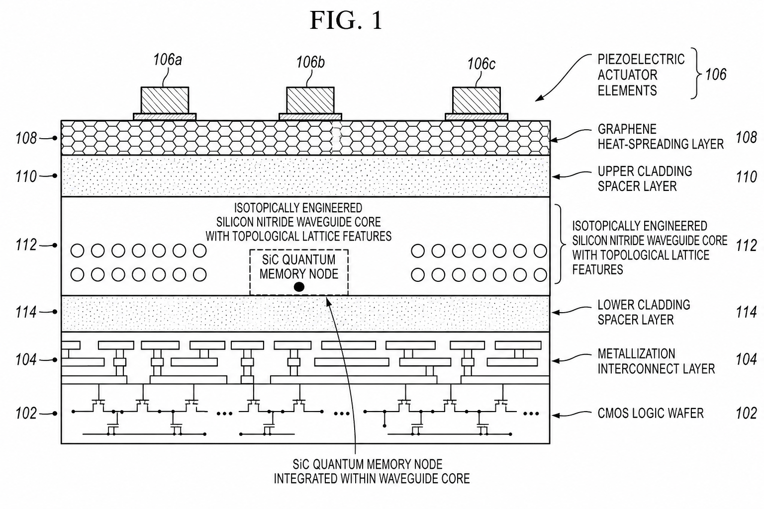
FIG. 1 — Cross-section of monolithic photonic-electronic SoC showing CMOS logic wafer, metallization, isotopically engineered Si₃N₄ core with SSH lattice, and graphene heat-spreading layer
Monolithic SoC Integration (100–112)
The CMOS logic wafer (102) with Cu/Al metallization (104) provides the electronic foundation. A planarized lower SiO₂ cladding supports the deuterated Si₃N₄:D core configured as an SSH topological lattice with alternating 0.15/0.25 µm interstitial gaps. A monolayer graphene heat spreader sits ≥2.0 µm above the core, ensuring <0.1% modal overlap while providing 5000 W/m·K lateral thermal conductivity.
SiC Nodes + PZT Phase Control
Silicon carbide quantum memory nodes with deterministically implanted defect centers are embedded within the isotopic dielectric environment, achieving T₂ coherence >1.5 ms at 300 K through anneal-free activation enabled by the isotopic shift. Piezoelectric (PZT) stress-optic actuators induce refractive index changes via mechanical strain at <1 nW power consumption and 200 ns response time — five orders of magnitude below thermal heaters.
Key performance parameters
| Parameter | Specification | Significance |
|---|---|---|
| Core Material | Si₃¹⁵N₄:D (deuterated) | Shifts parasitic overtones from C-band to 2100 nm |
| Propagation Loss (thin core) | 1.77 dB/m (0.177 dB/cm) | Qi = 14.9 million; enables 500+ gate operations |
| Topological Protection | SSH lattice, ±41 nm tolerance | Edge states immune to fabrication disorder up to 41 nm |
| SSH Gap Configuration | g₁ = 0.15 µm, g₂ = 0.25 µm | Coupling matrix ratio 0.17; establishes photonic bandgap |
| SiC Quantum Memory T₂ | >1.5 ms at 300 K | Room-temperature coherence for synchronization & error correction |
| PZT Actuator Power | <1 nW per phase shifter | 5 orders of magnitude below thermal heaters (10–50 mW) |
| Graphene Thermal Conductivity | >5000 W/m·K (in-plane) | Positioned ≥2 µm above core; <0.01 dB/cm added loss |
| End-to-End Loss Budget | 20 dB (19.76 dB allocated) | Supports >500 sequential logic gates with OPC correction |
| Fabrication Temperature | 250–350°C (BEOL compatible) | Monolithic integration on pre-processed CMOS logic wafers |
| Loss Per Photon Threshold | <2.7% per component | Below fault-tolerant threshold for dual-rail fusion-based QC |
Why this matters
±41 nm Defect Tolerance
The SSH topological lattice creates protected edge states that route photons around fabrication defects — width variations up to ±41 nm become non-events. Signal extinction ratio maintained >30 dB despite lithographic imperfections that would destroy conventional waveguide coherence.
1.77 dB/m Propagation
Deuterated core achieves Qi = 14.9 million (TM mode, 80 nm core). Passive routing consumes only 3.54 dB over 20 cm path length — just 18% of the total 20 dB system budget — leaving 82% available for active functional components that provide computational value.
Integrated SiC Quantum Memory
On-chip SiC quantum memory nodes with T₂ >1.5 ms at 300 K store photonic qubits for synchronization and error correction. Monolithic anneal-free activation via isotopic shift bypasses the 800–1200°C cycles required by conventional diamond NV centers.
Sub-Nanowatt Phase Control
PZT stress-optic actuators consume <1 nW per phase shifter with 200 ns response time. A processor with thousands of actuators operates within standard enterprise power budgets — eliminating thermal crosstalk that destabilizes quantum states in thermo-optic architectures.
Graphene Heat Spreading
Monolayer graphene (5000 W/m·K) positioned ≥2.0 µm above the core provides exceptional lateral heat dissipation from PZT actuators and OPC pump regions. Modal overlap <0.1% ensures <0.01 dB/cm added loss — active thermal management without optical penalty.
Back-End-of-Line Compatible
All fabrication at 250–350°C preserves Cu/Al metallization integrity. The photonic circuit sits directly above finished CMOS logic wafers — enabling monolithic photonic-electronic SoC with minimal signal latency between optical quantum processing and electronic classical control.
Built on established science
SSH Model Experimentally Validated
Su-Schrieffer-Heeger topological lattices have been demonstrated at MIT, Stanford, and multiple international groups. Protected edge states within photonic bandgaps are well-established physics — QLT applies the known framework to quantum computing routing networks.
Published Loss Reduction (Bose et al. 2024)
Anneal-free deuterated Si₃N₄ waveguides achieving 1.77 dB/m (Qi = 14.9M) published in Light: Science and Applications. The isotopic substitution strategy shifts Si–D and N–D overtones to 2100 nm, eliminating C-band absorption without high-temperature annealing.
Commercial PZT/AlN Maturity
PZT and AlN piezoelectric phase shifters are commercially available and used in existing photonic integrated circuits (arXiv 2603.02584, 2026). Sub-nanowatt operation with 200 ns response demonstrated — orders of magnitude improvement over thermal tuners.
Proven Thermal Management
Monolayer graphene transfer onto photonic structures is a mature technique. In-plane thermal conductivity of ~5000 W/m·K verified across multiple studies. Controlled separation from optical core prevents absorption while enabling efficient lateral heat dissipation.
Connected patent architecture
Room-Temperature Photonic Quantum Processor
Patent 05 provides the ultra-low-loss, fabrication-tolerant routing backbone that makes Patent 01's processor architecture physically realizable at scale — routing loss of just 3.54 dB across 20 cm enables the full 500+ gate depth.
View Patent →Self-Phase-Matched Hybrid Nonlinear Waveguide
Patent 02's OPC waveguide sections are integrated within Patent 05's topological routing network. The thick-core (800 nm) configuration supports nonlinear interactions while the thin-core (80 nm) handles long-haul routing at 0.177 dB/cm.
View Patent →Periodic OPC Lattice Method
Patent 08's periodic optical phase conjugation modules consume 9.0 dB of Patent 05's 20 dB loss budget but enable phase error correction that extends circuit depth from ~100 to 500+ gates — the loss-for-coherence tradeoff that makes deep quantum circuits viable.
View Patent →Self-Calibration & Predictive Health Monitoring
Patent 12's dual-use OPC diagnostic methods leverage Patent 05's integrated monitoring infrastructure to detect waveguide degradation, thermal drift, and actuator aging — enabling predictive maintenance of the quantum processor.
View Patent →The defect-tolerant foundation
Patent 05 provides the fabrication-robust circuit platform that makes QLT's processor (Patent 01) manufacturable at scale. While Patent 02 provides the nonlinear engine and Patent 04 provides mechanical reliability, Patent 05 ensures the entire routing network is immune to fabrication variations — achieving 1.77 dB/m loss with topological protection against ±41 nm defects, all at room temperature.